OPTICAL SHEET
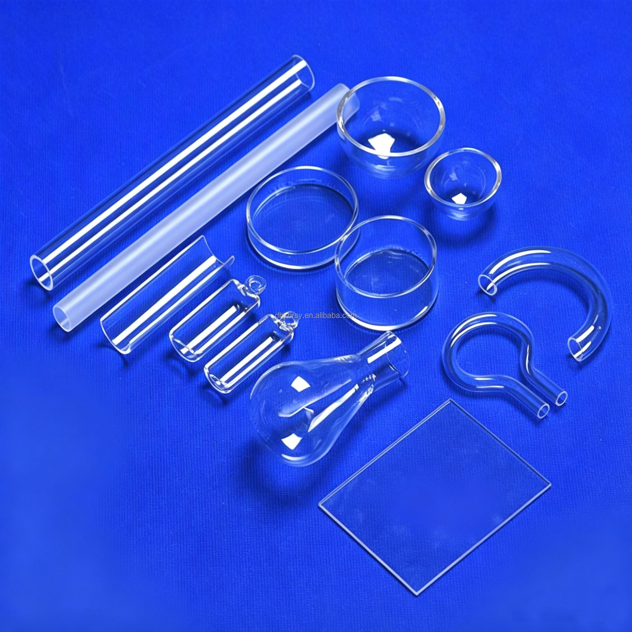
Engineered for extreme thermal shock, plasma etch resistance, and ultra-wide spectral transmission. Direct factory pricing with full material chemical analysis reports.
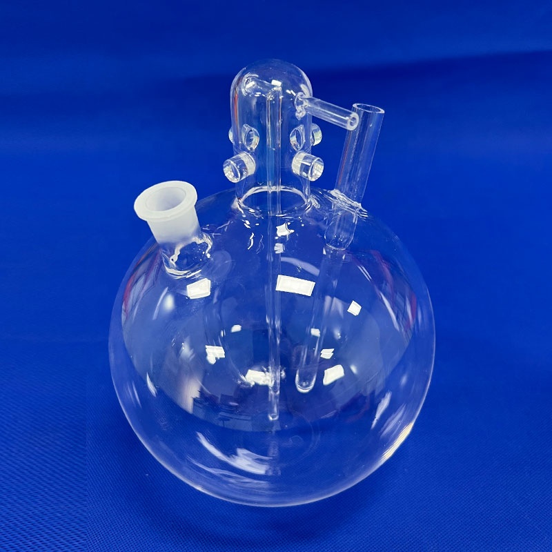
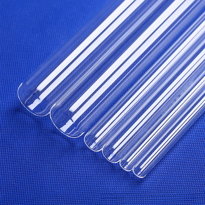
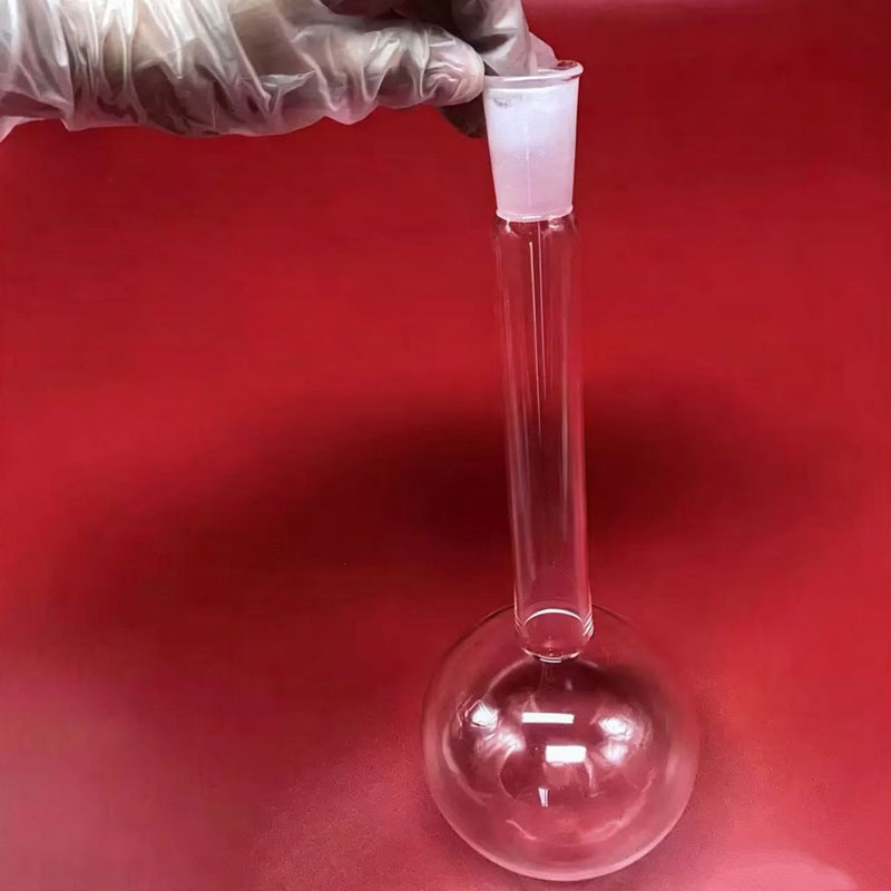
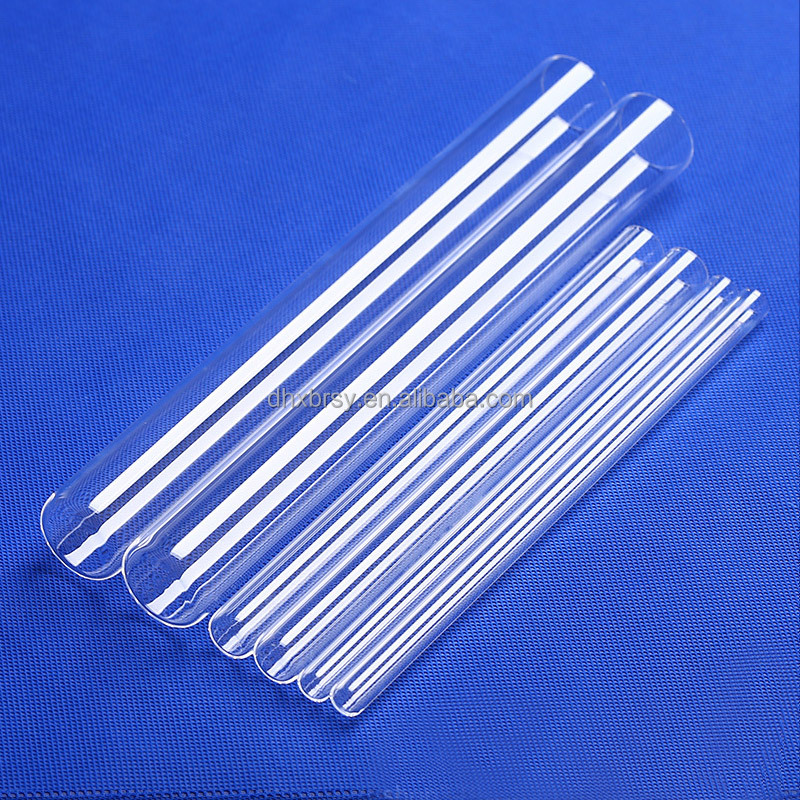
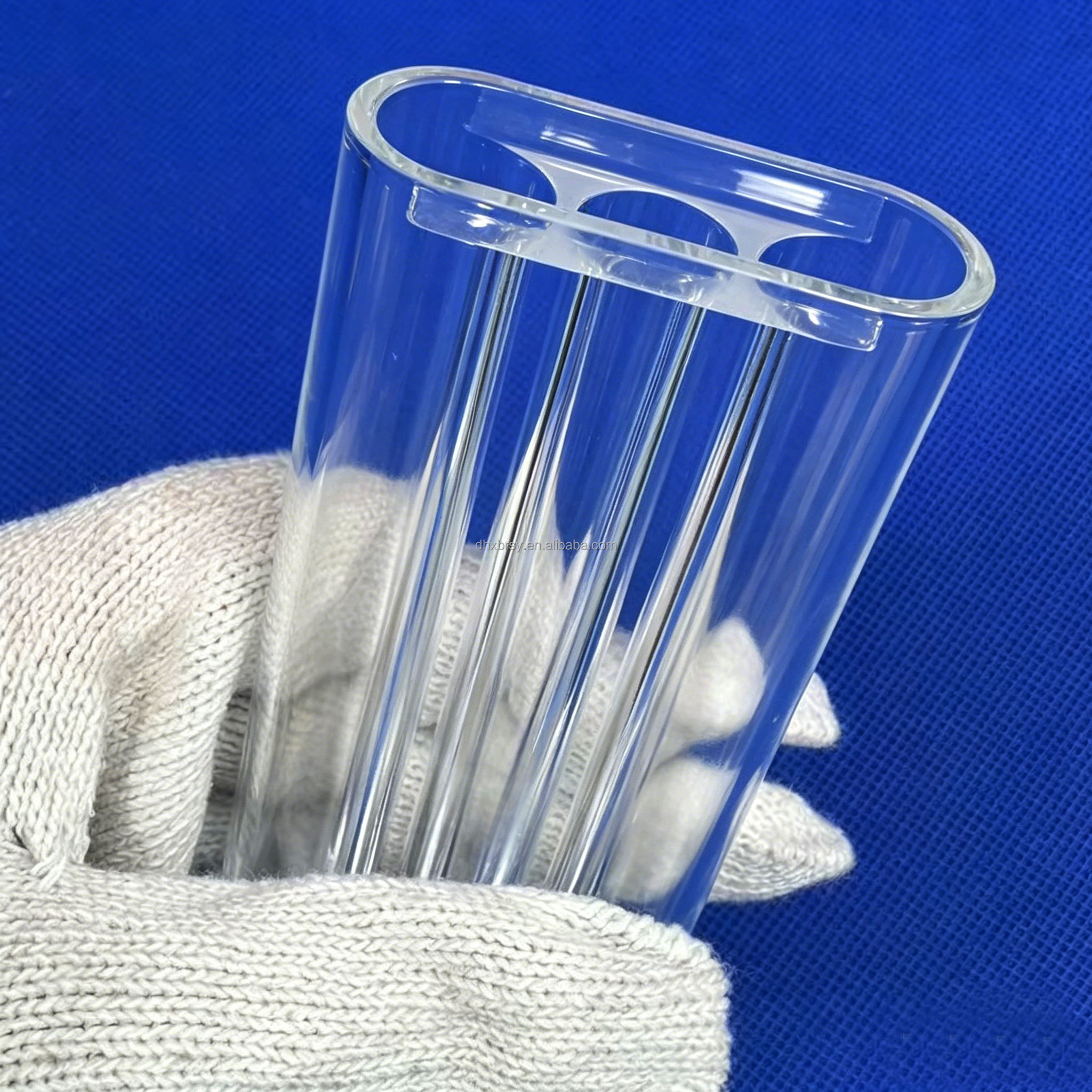
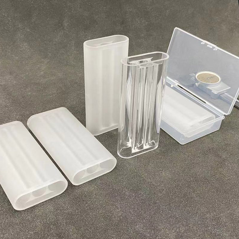
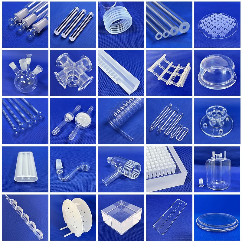
Understand atomic morphology, impurity control metrics, and transmission bands to prevent vacuum failures and optical degradation.
Synthesized through chemical vapor deposition of silicon halides with oxygen. It exhibits exceptional deep ultraviolet transparency down to 185 nm without solarization. With hydroxyl content controlled to < 5 ppm, it is critical for excimer lasers, DUV lithography optics, and ultra-high-precision semiconductor inspection.
Formed through high-temperature oxyhydrogen flame fusion of purified natural quartz crystal sand. Transmits cleanly from 220 nm to 2500 nm. JGS2 represents the industry workhorse for viewports, UV sterilization lamps, CVD process observation windows, and medical instrumentation where high transmission and structural rigidity intersect.
Electrically fused in vacuum environments, driving hydroxyl (OH⁻) ions down to undetectable levels (< 2 ppm). This virtually eliminates the 2.73 μm absorption band, enabling seamless transmission from 260 nm far into the mid-infrared up to 3500 nm. Ideal for pyrometry viewports, IR laser heaters, and analytical flow cells.
| Material Property | JGS1 (Synthetic Silica) | JGS2 (Oxyhydrogen Fused) | JGS3 (Electric Vacuum Fused) | Inspection Standard |
|---|---|---|---|---|
| SiO₂ Purity Level | ≥ 99.999% | ≥ 99.99% | ≥ 99.98% | ICP-OES Spectrometry |
| Transmission Spectrum | 185 nm – 2500 nm (Deep UV) | 220 nm – 2500 nm (Standard Optical) | 260 nm – 3500 nm (Infrared) | UV-Vis-NIR Spectrophotometer |
| Hydroxyl (OH⁻) Content | < 5 ppm – 1200 ppm (Grade dep.) | 150 – 300 ppm | < 2 ppm (OH-Free) | FTIR Infrared Absorption |
| Coefficient of Thermal Expansion | 5.5 × 10⁻⁷ / °C (20–300°C) | 5.5 × 10⁻⁷ / °C | 5.4 × 10⁻⁷ / °C | Dilatometry (ASTM E228) |
| Maximum Working Temp (Continuous) | 1150 °C | 1100 °C | 1150 °C | High Temp Anneal Test |
| Surface Roughness Capability | Ra ≤ 0.2 nm (Super-Polished) | Ra ≤ 0.5 nm (CMP Grade) | Ra ≤ 0.8 nm (Standard Polish) | Atomic Force Microscopy (AFM) |
How semiconductor node shrinkage, EUV lithography, and photovoltaic N-type cell transitions are redefining technical sourcing requirements.
Sub-5nm semiconductor fabs can no longer tolerate classic semiconductor-grade quartz. Trace elements like Lithium (Li), Sodium (Na), Potassium (K), and Iron (Fe) act as mobile gate contaminants. Global procurement is shifting directly towards multi-stage acid-leached high-purity natural silica sand (> 99.998%) with cumulative trace metallic impurities held strictly below 8 ppm.
Photovoltaic TOPCon and HJT cell production requires massive tube chambers and rectangular quartz sheets up to 800 mm × 1200 mm. Maintaining structural integrity, parallelism (< 0.02 mm), and zero sagging during prolonged 1150°C thermal oxidation drives the transition to hot isostatically pressed (HIP) dense silica structures with optimized viscosity parameters.
High-energy laser optical systems demand rigorous polarization testing. Conventional visual checks are replaced by strict automated polariscopic inspection verifying optical path difference (OPD) ≤ 5 nm/cm. Annealing ovens with precision cooling gradients under computer PID control ensure that thermal residual stresses never induce in-situ fracture during pulse laser strikes.
Operating from China's primary quartz industrial base in Lianyungang, we oversee the full supply chain to eliminate intermediate distributor markups.
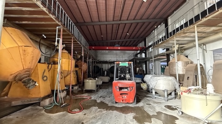
Crushed and screened silica crystals undergo prolonged multi-acid washing to leach out trace metallic contaminants, securing 99.99% core purity.
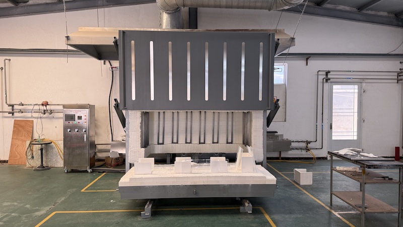
Fusion products are soaked at 1215°C and gradually brought down to room temperature to release structural tension and eliminate micro-fissuring.
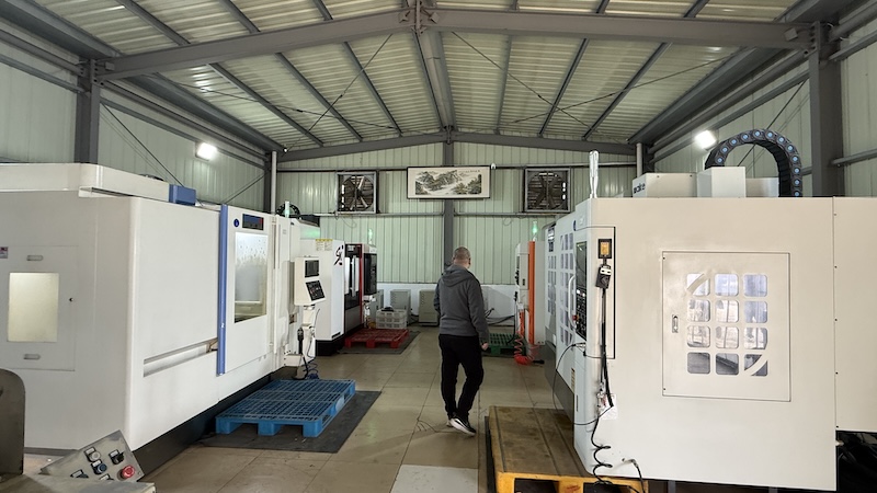
Diamond tooling enables complex CNC boring, slotting, water-jet slicing, beveling, and step milling to micron-level customer CAD tolerances.
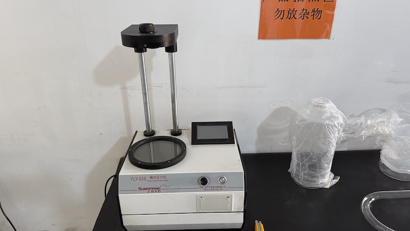
Every delivery batch is certified using cross-polarization stress testers, laser interferometers, and dimensional coordinate measuring machines (CMM).
Headquartered in Tuofeng Industrial Park, Lianyungang, Jiangsu, Lovri Quartz leverages direct regional access to premier silica deposits and an advanced manufacturing cluster. As an SGS-verified manufacturer across 14,271 m² of production infrastructure, we bridge material science with precision optical fabrication.
Send your 2D/3D mechanical drawings (PDF, DWG, STEP) for rapid DFM evaluation and transparent volume quotations within 12 hours.
Contact UsClear, technically accurate answers to mitigate international procurement risks, customs clearance concerns, and engineering verification issues.
Connect with our technical sales engineers to review tolerances, material grades, and obtain volume-discounted quotes.
Contact Us