Featured High-Purity Fused Silica & Quartz Products
Direct from our SGS-verified fabrication center: ultra-thin sheets, semiconductor digestion tubes, laser reactors, and optical components manufactured to micron-level tolerances.
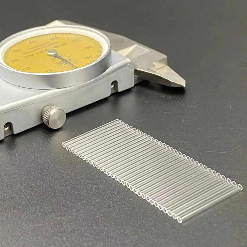
BAO RAN 419 Ultra-Thin 0.1mm–0.5mm Quartz Sheet (99.99% SiO2)
- Thickness: 0.1, 0.2, 0.3, 0.4, 0.5 mm
- Surface Roughness: Ra < 0.5 nm
- ROHS Certified & Laser-Ready
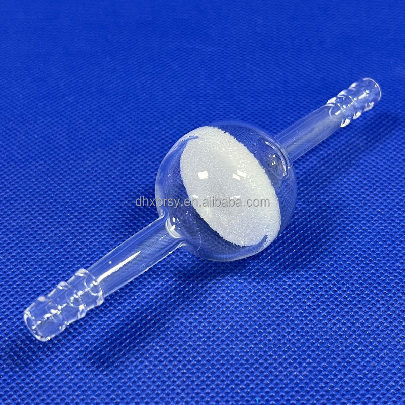
High Purity Transparent Fused Quartz Sheet & Digestion Tube
- Heat Resistance: Up to 1200 °C continuous
- Light Transmittance: > 92% in visible band
- Customized Laboratory Digestion Geometry
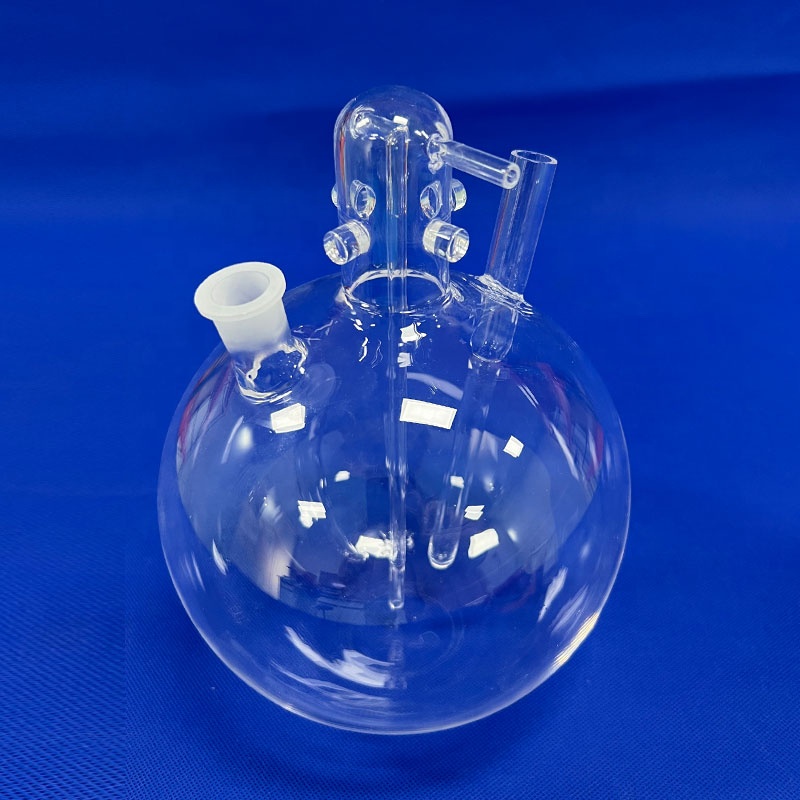
High-Purity SiO2 Quartz Glass Reactor for Laser Machinery
- Purity: 99.99% Electronic Grade Silica
- CNC Machined Chamber Ports
- Bubble-free & Low Internal Stress

Clear Fused Silica Tube with Closed Bottom for Semiconductor
- OD/ID Tolerance: Within ±0.05 mm
- Chemical Inertness against mineral acids
- Flat or Dome Bottom Flame Sealing
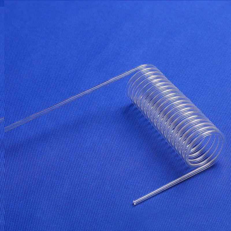
Fused Quartz Spiral Tube for High-Intensity Laser Equipment
- Precision Bending & Flame Polishing
- Selective Wavelength Transmission
- Fully RoHS Compliant Substrate
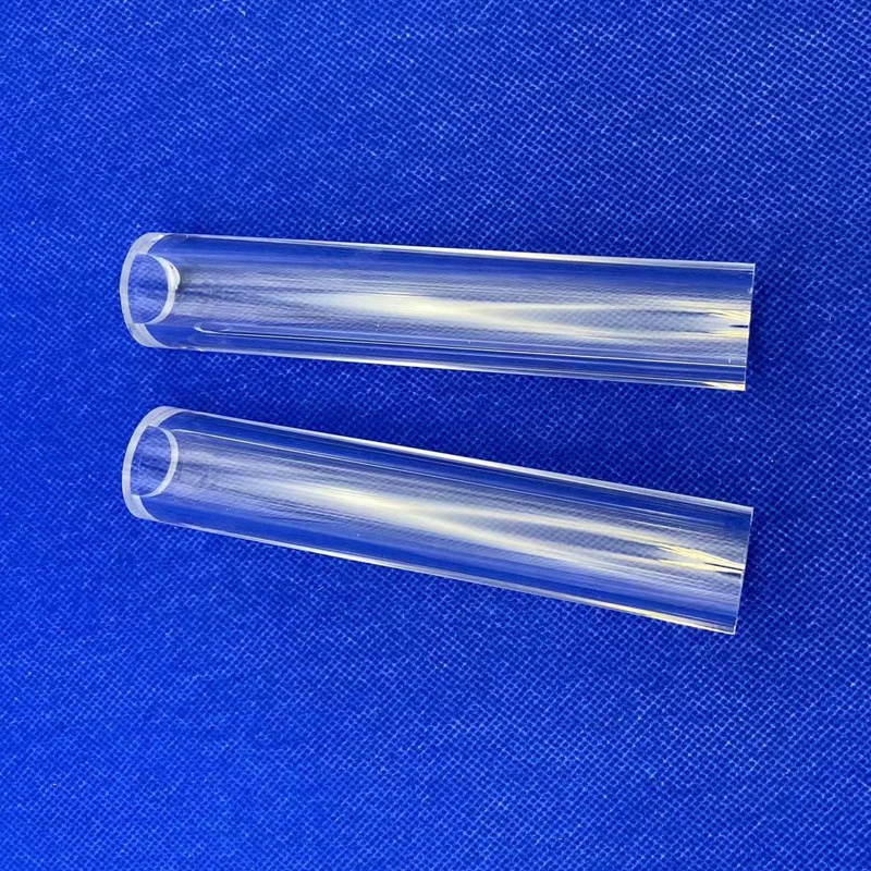
High Precision Quartz Tube for Ozone & Far-Infrared Heaters
- Dielectric Strength: High breakdown barrier
- Thermal Shock: Delta 1100 °C to water safe
- Precise Dimensional Concentricity
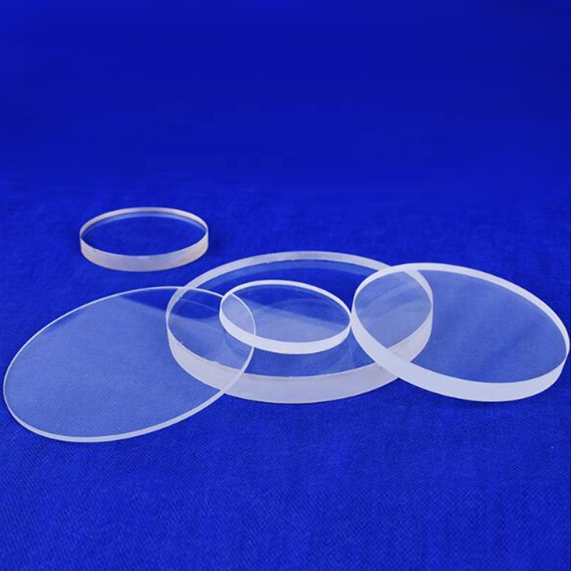
Double-Sided Polished Fused Quartz Disc & Wafer Substrate
- Flatness: Lambda/4 to Lambda/10 per inch
- Scratch-Dig: 20-10 / 10-5 Laser Quality
- TTV < 2 μm for 100mm–300mm wafers
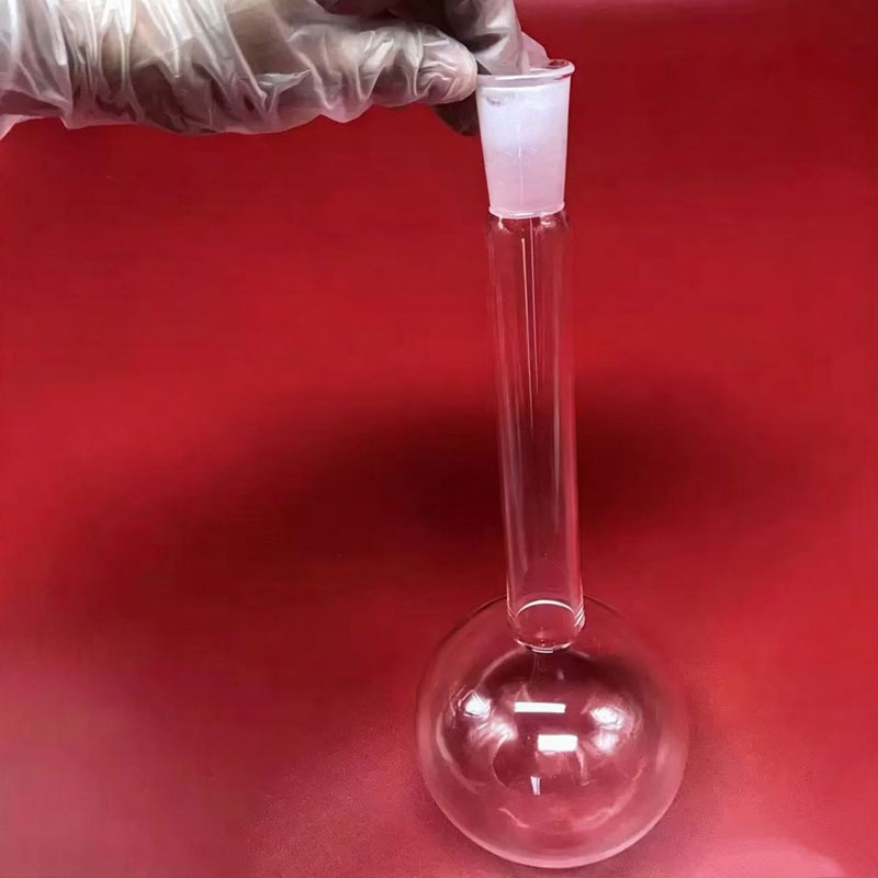
1200-Degree Corrosion-Resistant Quartz Glass Long-Neck Flask
- 99.99% SiO2 High-purity Raw Batch
- Annealed to Zero Internal Residual Stress
- Resistance to Aqua Regia & Halogens
1. The Critical Role of Fused Silica Wafers in Modern Microelectronics
In high-frequency telecommunications, micro-electro-mechanical systems (MEMS), photonic integrated circuits (PICs), and advanced lithography tooling, standard monocrystalline silicon or borosilicate glass often encounters profound physical limitations. Fused silica wafers (vitreous silicon dioxide, SiO2) provide an indispensable combination of near-zero thermal expansion (0.55 × 10⁻⁶ / °C), extreme optical transmission spanning the deep ultraviolet (DUV 185 nm) through mid-infrared (MIR 3500 nm), exceptionally low dielectric loss (loss tangent < 0.0004 at 10 GHz), and superior electrical insulation properties.
Unlike standard borosilicate glasses (e.g., Pyrex or Schott Borofloat), fused silica consists entirely of pure silicon and oxygen tetrahedra in an amorphous, non-crystalline matrix. The absence of alkali network modifiers (such as sodium, boron, or potassium) yields a dielectric constant (εr ≈ 3.8 at 1 MHz) that remains rock-solid across wide thermal excursions up to 1000 °C. For semiconductor fabrication engineers, this translates to minimal substrate parasitic capacitance, virtually non-existent RF attenuation in high-speed RFIC carriers, and exceptional thermal-shock resistance during plasma-enhanced chemical vapor deposition (PECVD) and reactive ion etching (RIE) cycles.
Material Classification: Synthetic Fused Silica vs. Natural Fused Quartz
A vital distinction in wafer procurement lies between synthetic fused silica (typically designated as JGS1 or excimer-grade) and natural fused quartz (JGS2 and JGS3 grades):
- Synthetic Fused Silica (JGS1 / Suprasil / HPFS): Synthesized via chemical vapor deposition (CVD) or flame hydrolysis of silicon tetrachloride (SiCl4) or siloxane precursors. This grade is virtually free of metallic contaminants (total heavy metals < 0.1 ppm) and exhibits zero bubble inclusions. It provides uncompromised transmission down to 185 nm, rendering it the standard for DUV stepper photomasks, excimer laser windows, and laser damage threshold (LIDT) optics.
- Fused Natural Quartz (JGS2 / Optosil): Produced by electric-arc or oxy-hydrogen flame fusion of naturally occurring high-purity quartz crystals (silica sand). While exhibiting outstanding mechanical, thermal, and dielectric performance, it features trace metallic impurities (Al, Fe, Ti, Li) in the parts-per-million regime and absorption bands at 245 nm and 2.73 μm (hydroxyl OH⁻ bond). It is broadly utilized as wafer carriers, RF sputtering substrates, furnace process discs, and sight glasses.
- Water-Free Infrared Fused Silica (JGS3 / Infrasil): Electrically fused under low-pressure vacuum to strip hydroxyl ions (OH⁻ content < 5 ppm). This eliminates the prominent 2.73 μm absorption dip, delivering sustained transparency across the short-to-mid infrared spectrum up to 3.5 μm.
2. Technical Benchmark: Material Grades for Wafer Substrates
Before selecting a manufacturing partner, review the essential mechanical, thermal, and optical properties that dictate yield in wafer-level packaging (WLP) and lithography:
| Property Parameter | JGS1 (Synthetic Fused Silica) | JGS2 (Optical Fused Quartz) | JGS3 (Infrared Fused Quartz) | Borosilicate Glass (Reference) |
|---|---|---|---|---|
| SiO2 Purity | ≥ 99.999% (< 0.1 ppm metals) | ≥ 99.99% (≤ 10 ppm metals) | ≥ 99.99% (≤ 15 ppm metals) | ≈ 81% SiO2 (with B2O3, Na2O) |
| Transmission Range | 185 nm – 2500 nm | 220 nm – 2500 nm | 260 nm – 3500 nm | 350 nm – 2000 nm |
| OH⁻ (Hydroxyl) Content | 100 – 1200 ppm (High OH) | 30 – 200 ppm | < 5 ppm (Water-Free) | Not Applicable |
| Thermal Expansion (CTE) | 0.55 × 10⁻⁶ / K | 0.55 × 10⁻⁶ / K | 0.55 × 10⁻⁶ / K | 3.25 × 10⁻⁶ / K |
| Softening Point | 1730 °C | 1710 °C | 1710 °C | 820 °C |
| Dielectric Constant (εr at 1 MHz) | 3.80 | 3.82 | 3.82 | 4.60 |
| Loss Tangent (tan δ at 1 GHz) | < 0.0001 | ≈ 0.0003 | ≈ 0.0003 | ≈ 0.0035 |
| Surface Roughness (CMP Ra) | < 0.3 nm (Super-Polished) | < 0.5 nm | < 0.5 nm | ≈ 0.8 – 1.2 nm |
3. Comprehensive Analysis: Top 10 Fused Silica Wafer Manufacturers & Suppliers
Navigating the global supply chain requires distinguishing between raw ingot synthesizers, precision double-side polishing (DSP) houses, and full-chain OEM fabricators. The following 10 enterprises represent the pinnacle of engineering capability, quality assurance, and commercial reliability in 2025/2026.
4. Future Procurement Trends in Fused Silica Substrates (2025–2030)
As microelectronics enters the post-Moore era and quantum technologies mature, procurement strategies for fused silica substrates are undergoing radical shifts. Sourcing directors must anticipate the following four market-defining transformations:
Transition to 300 mm Glass Core Substrates
Traditional organic build-up substrates (ABF) are reaching thermal and dimensional limits in advanced 2.5D/3D packaging. Leading chipmakers are rapidly introducing 300 mm fused silica and high-purity glass core substrates for high-density interposers, demanding sub-micron Total Thickness Variation across 12-inch formats.
Laser-Induced Deep Etching (LIDE) & TGV
Mechanical diamond drilling of brittle fused silica induces micro-cracks and sub-surface damage. Procurement contracts increasingly mandate Laser-Induced Deep Etching (LIDE) to achieve micro-through-glass vias (TGVs) with pitch dimensions under 50 μm and aspect ratios exceeding 10:1 without thermal fractures.
Sub-ppb Metallic Purity for Fusion Bonding
Direct low-temperature hydrophilic fusion bonding of silica wafers to silicon or gallium nitride (GaN) requires zero metallic migration. Fab lines now impose rigorous Inductively Coupled Plasma Mass Spectrometry (ICP-MS) limits: Na, Ca, Fe, and Cu concentrations must each verify below 0.1 ppb to prevent threshold drift.
Dual-Sourcing & Decoupled Supply Redundancy
Geopolitical tariffs and energy supply disruptions have made single-source dependence on Western conglomerates hazardous. Procurement directors are systematically qualifying agile Chinese source manufacturers—such as Lovri Quartz—as verified tier-2 and primary OEM partners to ensure stable production economics.
5. Technical Sourcing FAQ: Critical Engineering Questions Answered
Consult these authoritative engineering explanations addressing common fabrication anomalies, surface finish metrics, and specification pitfalls:
What is the practical difference between JGS1, JGS2, and JGS3 quartz in wafer fabrication?
How do Total Thickness Variation (TTV), Bow, and Warp impact semiconductor yield?
Why is polarization stress inspection mandatory before wafer slicing and delivery?
Can ultra-thin fused silica wafers (0.1 mm – 0.3 mm) survive automated robotic cassette handling?
What export packaging protocols are required to avoid surface contamination and transit breakage?
Why Tier-1 Engineers Partner with Lovri Quartz
Located in the heart of Lianyungang's global quartz mineral hub, Lovri Quartz Products Co., Ltd. operates a modern, 14,271 m² manufacturing complex assessed and certified onsite by SGS Group. We eliminate intermediary markups and deliver uncompromising engineering support from single-piece prototyping to high-volume semiconductor fab supply.
Support for customer CAD formats: STEP, DWG, DXF, or PDF engineering prints reviewed within 12 hours.
Request Engineering Review
Connect immediately with our technical quartz fabrication team to evaluate tolerances, substrate grades, and production lead times.
Get a Quote