Featured High-Purity Fused Quartz & Silica Solutions
Precision-engineered fused silica substrates, customized furnace assemblies, and optical-grade components built to strict ISO/RoHS tolerances.
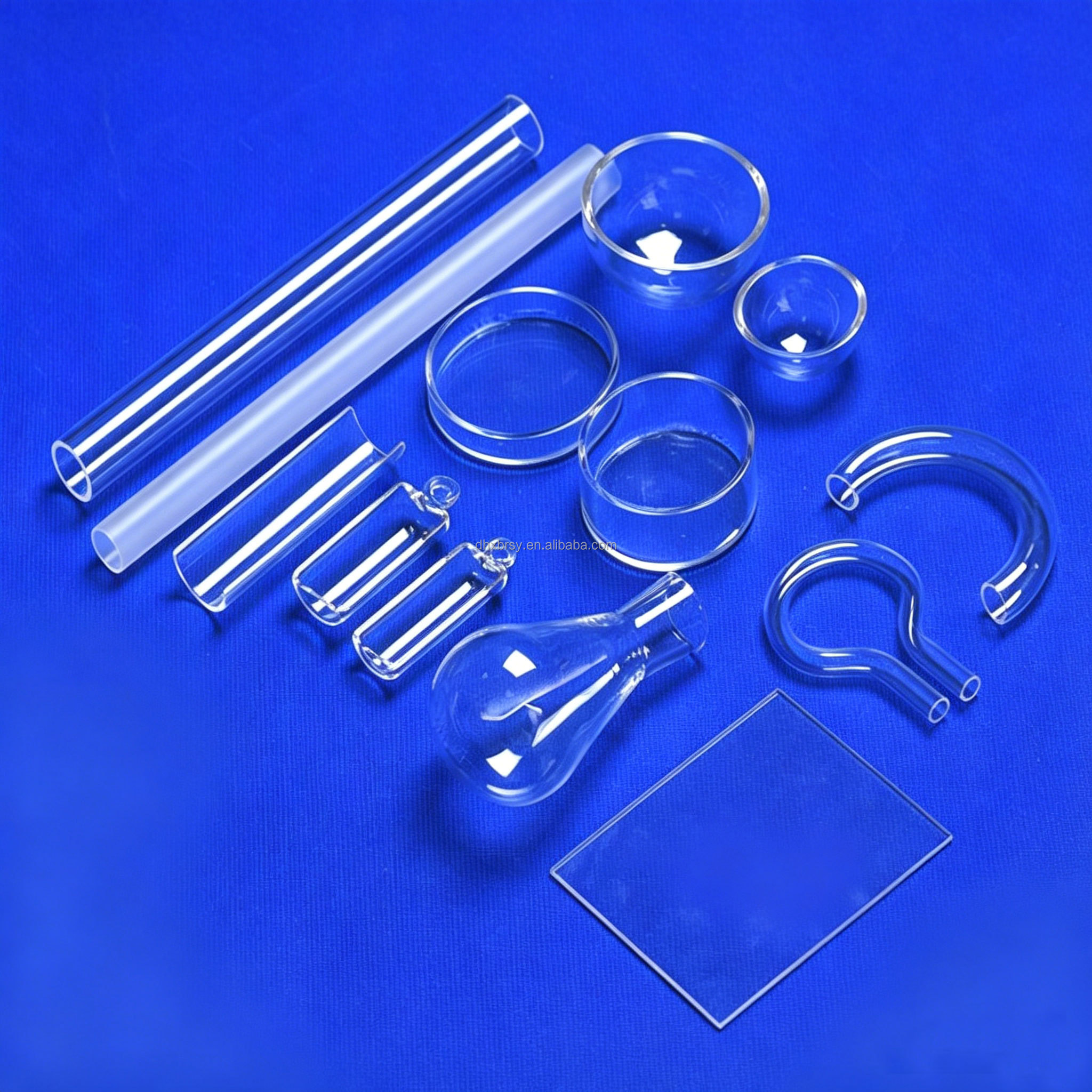
Custom Lab Quartz Glass Apparatus High Purity 99.99% Silica Content ROHS Certified Semiconductor Manufacturing OEM ODM
Application: Semiconductor Etch & Diffusion Systems
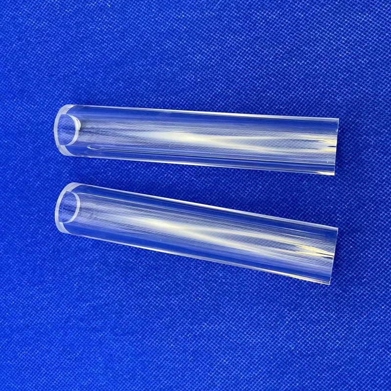
High Precision Clear Quartz Glass Tube Fused Silica High Quality Bending Welding Cutting Ozone Generator Far-infrared Heaters
Capability: Flame Welding, Custom Flanges
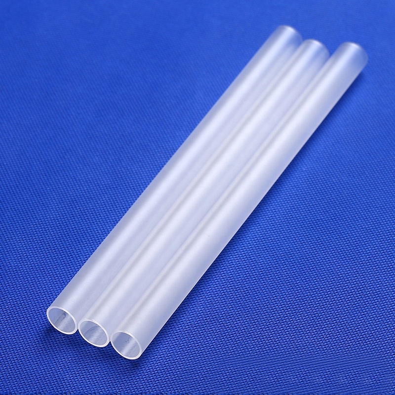
High Purity Translucent Polished Quartz Glass Tube Welding Bending Cutting High Ozone Ozone Generator Lab Infrared Heating UV
Feature: High Deep-UV (185nm/254nm) Efficiency
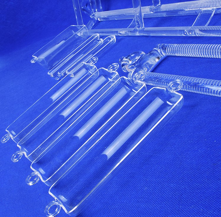
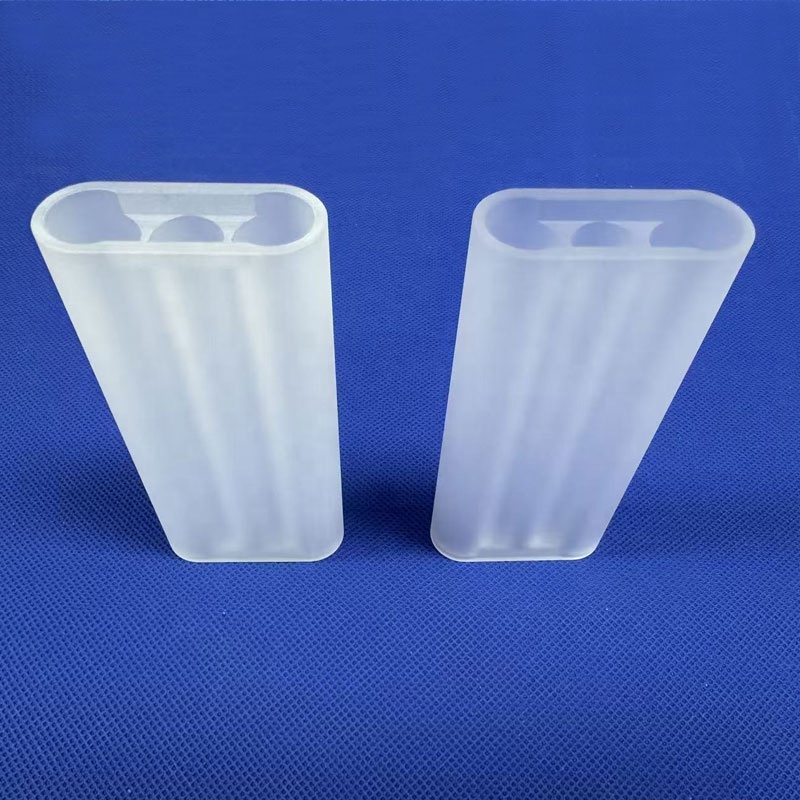
BRO RAN High Precision Triple Bore Quartz Glass (SiO2) 200 Mesh Laser Cavity Flow Tube for GentleYag/GentleMax Hair Removal
Application: Medical Nd:YAG Laser Systems
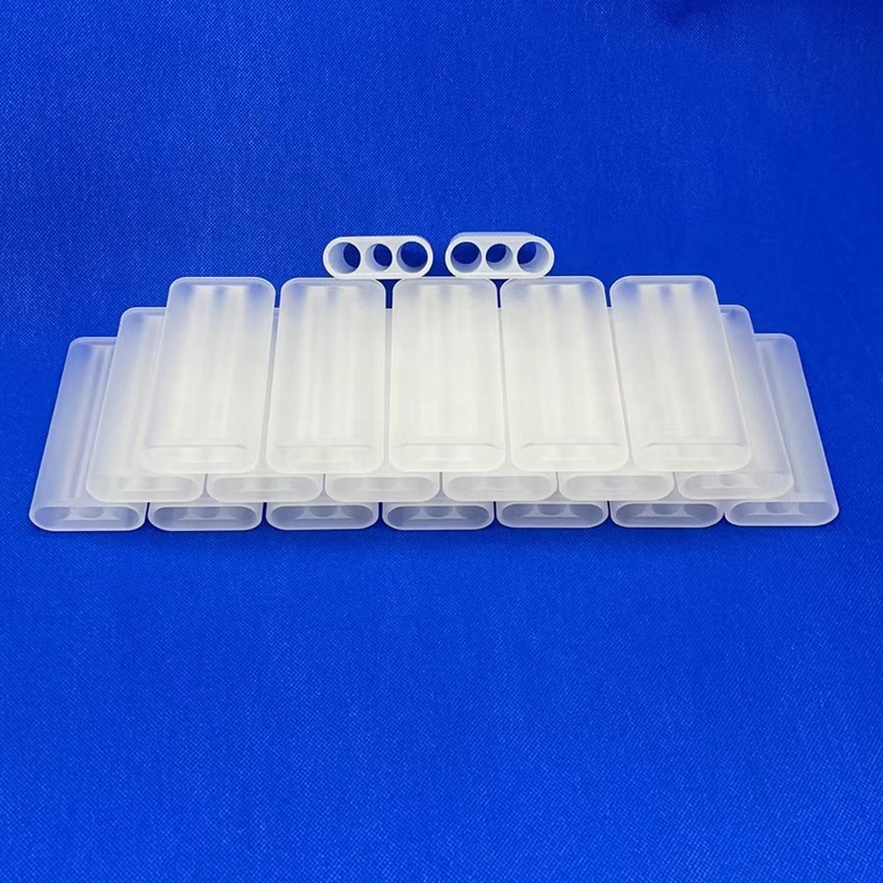
Quartz Triple Bore Flow Tubes Laser C Shape Fused Quartz Welding Bending Cutting Services 99.98% Silica Content ROHS Certified
Quality: 100% Polarization Stress Tested
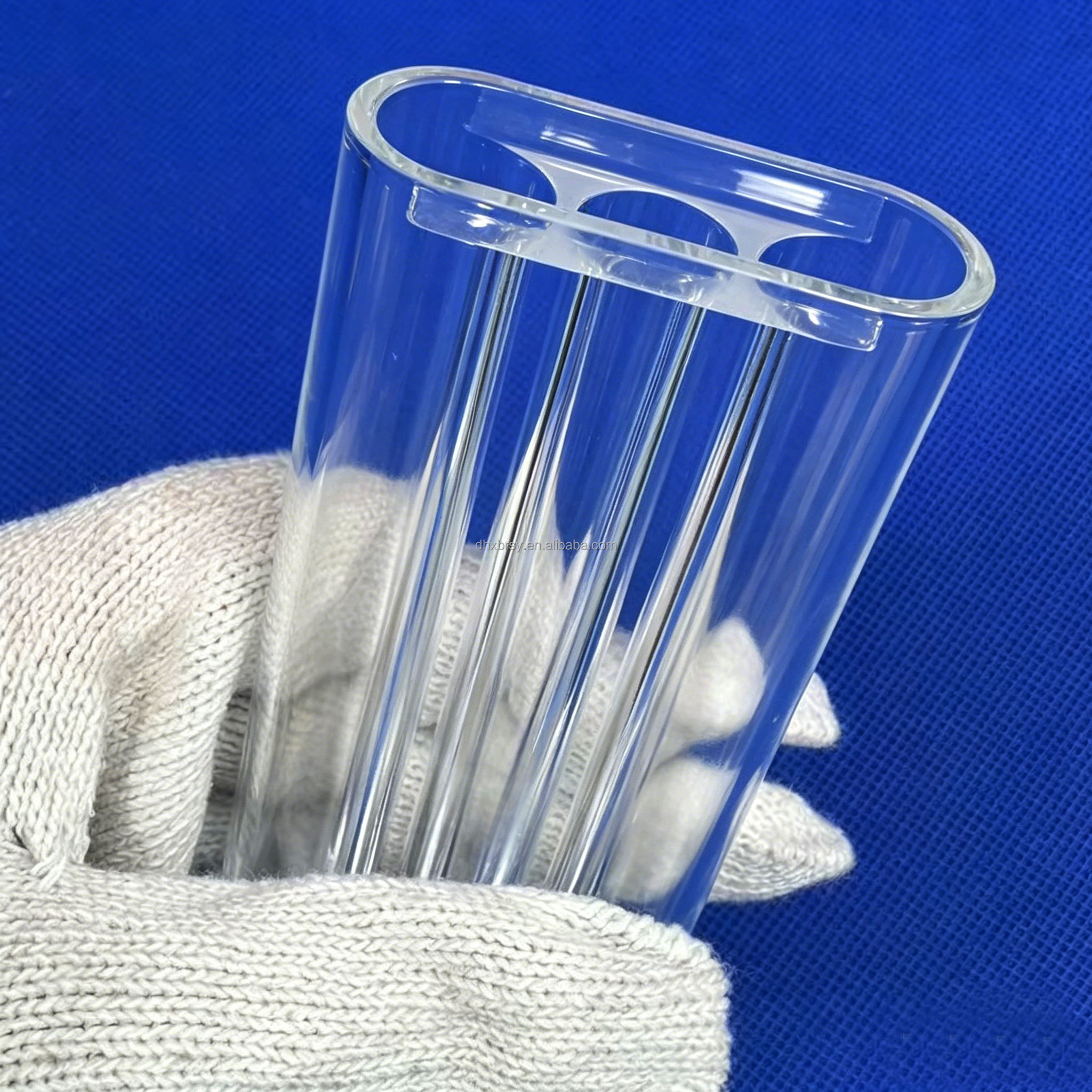
916Factory Customized Quartz Glass Tubes High Temperature Fused Silica Quartz Glass Tube for Lab Furnace Semiconductor Industry
Thermal Limit: 1300 °C Intermittent Operation
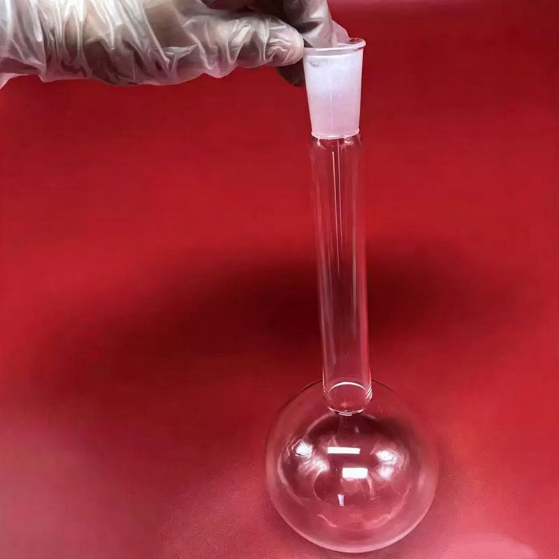
99.99% High-purity SiO2 High-temperature Resistant 1200-degree Corrosion-resistant ROHS Certified Quartz Glass Long-neck Flask
Annealing: Uniform Thermal Expansion Coefficient
1. The Strategic Role of Chinese Fused Silica Substrate Fabricators
Analyzing raw crystalline purity, electric vs. flame fusion processes, and optical transmission windows.
In precision engineering, wafer fabrication, UV lithography, and high-energy laser optics, the fused silica substrate remains an indispensable material cornerstone. Unlike conventional silicate glasses, amorphous silicon dioxide (SiO₂) delivers an extraordinary combination of near-zero thermal expansion coefficient (~5.5 × 10⁻⁷ /°C), superior ultraviolet-to-near-infrared optical transmission (185 nm to 2500 nm), and unmatched dimensional rigidity under severe thermal shock conditions. As global manufacturing demands tighter mechanical tolerances and lower contamination margins, China—specifically the specialized industrial cluster in Lianyungang, Jiangsu—has evolved into the world's primary manufacturing hub for high-yield, cost-effective, and fully certified fused quartz and synthetic fused silica components.
International optical design engineers and procurement officers frequently grapple with the technical nuances separating naturally fused quartz from synthetic fused silica. While naturally fused quartz (derived from high-grade quartz sand refined via electrical or oxyhydrogen flame fusion) provides exceptional mechanical strength and continuous resistance to thermal sagging at operating temperatures up to 1100 °C, synthetic fused silica (synthesized through the chemical vapor deposition or flame hydrolysis of silicon tetrachloride, SiCl₄) achieves near-zero metallic trace impurities (<0.1 ppm total metals) and eliminates refractive index variations. Selecting the optimal China fused silica substrate supplier requires in-depth visibility into factory-floor capabilities, raw material origins, annealing schedules, and optical inspection regimes.
JGS1: Synthetic Deep-UV
Synthesized via SiCl₄ vapor hydrolysis. Absolutely free of bubble inclusions with maximum transmission across 185 nm – 2500 nm. Essential for excimer laser lithography windows, DUV beam splitters, and aerospace sensors.
JGS2: Optical Flame-Fused
Melted using high-purity natural crystal sand in hydrogen-oxygen flames. Exhibits exceptional optical homogeneity over 220 nm – 2500 nm. The premier standard for precision sight windows, UV disinfection tubes, and lab viewports.
JGS3: Infrared Electrically Fused
Vacuum electrically fused quartz with virtually zero hydroxyl (OH⁻ < 2 ppm) content. Eliminates the notorious 2.73 μm absorption dip, delivering peak infrared performance up to 3500 nm for pyroelectric instruments and IR heaters.
2. Comprehensive Substrate Material & Fabrication Matrix
Benchmark comparative data for technical buyers evaluating mechanical, thermal, and optical parameters.
| Physical / Chemical Property | High-Purity Fused Silica (JGS1 / JGS2) | Semiconductor Quartz Glass | Borosilicate / Float Glass |
|---|---|---|---|
| SiO₂ Chemical Purity | ≥ 99.998% (Metals < 15 ppm) | ≥ 99.99% | 70% – 81% |
| Refractive Index ($n_d$) | 1.45846 @ 589.3 nm | 1.4585 | 1.5170 |
| Coefficient of Thermal Expansion (CTE) | 5.5 × 10⁻⁷ /°C (20 °C to 320 °C) | 5.4 × 10⁻⁷ /°C | 32.5 × 10⁻⁷ /°C to 85 × 10⁻⁷ /°C |
| Annealing Point / Softening Point | 1215 °C / 1730 °C | 1180 °C / 1680 °C | 560 °C / 820 °C |
| Thermal Shock Tolerance | ΔT > 1000 °C (Water Quench Proof) | ΔT > 950 °C | ΔT ≈ 150 °C (Cracks readily) |
| Surface Roughness (CMP Polishing) | Ra < 0.3 nm to 0.5 nm (Super-polished) | Ra < 1.0 nm | Ra > 2.5 nm |
| Total Thickness Variation (TTV) | < 1.5 μm across Ø200 mm Substrates | < 3.0 μm | > 15.0 μm |
| Dielectric Breakdown Strength | 25–40 kV/mm @ 20 °C | 20–30 kV/mm | 10–15 kV/mm |
3. Future Procurement Trends in Fused Silica Substrates (2025–2030)
Anticipating structural supply chain pivots, advanced lithography nodes, and optical interconnect demands.
The global procurement landscape for high-precision fused quartz and synthetic silica substrates is undergoing rapid structural evolution. B2B sourcing executives must account for five pivotal macro trends transforming supplier evaluations across North America, Europe, and Asia-Pacific:
Photomask Substrate Miniaturization
With semiconductor fabrication expanding into 3nm and 2nm gate-all-around (GAA) architectures, extreme requirements for zero-defect photomask blanks are forcing suppliers to eliminate nanometer-scale inclusions and subsurface micro-cracks through rigorous double-sided CMP polishing.
High-Power Laser Optical Damage Thresholds (LIDT)
Industrial multi-kilowatt fiber lasers and medical aesthetic platforms require fused silica substrates capable of withstanding LIDT > 10 J/cm² at 1064 nm with 10 ns pulses. Subsurface damage during CNC edge grinds must be eliminated via chemical acid etching relief.
Silicon Photonics & DWDM Packaging
Data center expansion driven by generative AI infrastructure demands high-density optical transceiver blocks. Synthetic fused silica microplates and capillary V-groove arrays provide the thermal dimensional stability necessary to align multi-fiber arrays with zero signal drift.
Integrated Factory Traceability & ESG
International OEMs are moving away from unregulated brokers. Long-term procurement agreements require full supply chain visibility, including raw silica pulverization records, acid-pickling wastewater compliance, and certified RoHS/REACH chemical documentation.
4. Breakthroughs in Fused Silica Production & Cold Machining
How top Chinese manufacturers combine hot-melt glassblowing with 5-axis ultrasonic CNC diamond profiling.
Historically, quartz glass components were restricted to simple cylindrical pipes, flat discs, and basic labware shaped through manual oxyhydrogen torch manipulation. Today, top tier China fused silica factories operate integrated facilities that bridge high-temperature pyrochemical synthesis with ultra-precise computer numerical machining (CNC).
Ultrasonic-Assisted 5-Axis CNC
High-frequency axial vibrations combined with electroplated diamond toolheads cut micro-cracking forces by up to 60%. This enables fragile multi-bore flow tubes, deep-grooved wafer boats, and micro-fluidic quartz channels without chipping.
Polarization Stress-Relief Annealing
Rapid thermal gradients during flame reshaping introduce frozen residual internal stresses. Factory-grade continuous programmable annealing cycles cool components precisely through the 1150 °C to 950 °C transformation zone to prevent unexpected thermal cracking.
Acid Pickling & Surface Passivation
Multi-stage hydrofluoric (HF) and nitric (HNO₃) acid immersion cleans quartz sand feedstocks while stripping subsurface micro-fractures induced by mechanical saws. This process increases structural flexural strength by more than 30%.
5. Enterprise Advantages of Lovri Quartz Products Co., Ltd.
Vertically integrated source manufacturing based in Tuofeng Industrial Park, Lianyungang, Jiangsu.
When evaluating Chinese suppliers, procurement risks often stem from trading intermediaries misrepresenting subcontracted workshops. Lovri Quartz Products Co., Ltd. stands apart as an SGS onsite-verified source manufacturer with a comprehensive 14,271 m² operational facility controlling every step of production.
True Source Material Control
By executing raw crystal lump sizing, automated pulverizing, magnetic separation, and high-concentration acid pickling within our own plant, we eliminate contaminated third-party quartz sand, guaranteeing 99.99% SiO₂ baseline purity.
Full-Cycle Precision CNC Machining
Equipped with computerized high-speed multi-axis mills, precision surface grinders, laser flow-tube cutters, and thread-cutting lathes capable of maintaining tight tolerances down to ±0.01 mm on custom flanges, disc substrates, and multi-bore tubes.
100% Polarization Stress Inspection
Every single manufactured apparatus, furnace tube, and polished plate passes an optical polariscope stress inspection prior to export packaging, ensuring that thermal-induced internal strain is completely neutralized.
Flexible MOQ & Safe Global Logistics
We actively support engineering R&D teams with prototyping minimum order quantities (from 1 to 5 pieces) alongside bulk container orders. Finished goods are secured in multi-layer shockproof PE foam and custom fumigated plywood crates.
6. Frequently Asked Questions (FAQ) for Global Buyers
Essential technical clarifications addressing specifications, lead times, optical certifications, and drawing reviews.