SGS Onsite-Verified Fused Quartz Manufacturer [email protected]

OEM/ODM Quartz Wafer Boat Manufacturer & Exporters for San Francisco

Precision 99.99% SiO₂ Thermal Carriers Engineered for Advanced Silicon Valley Foundries, R&D Cleanrooms, and NorCal Semiconductor Fabs

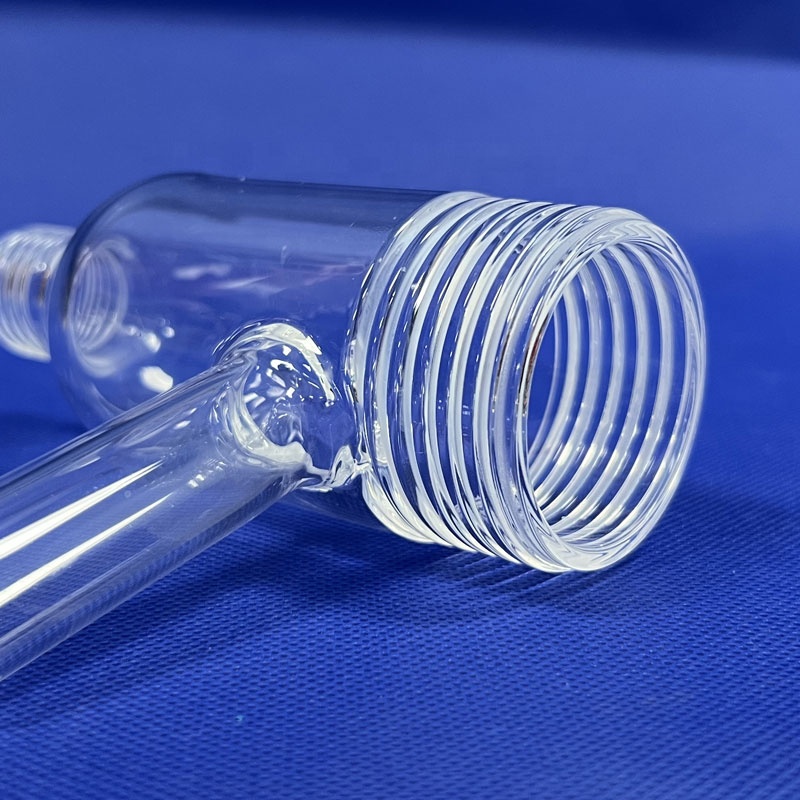
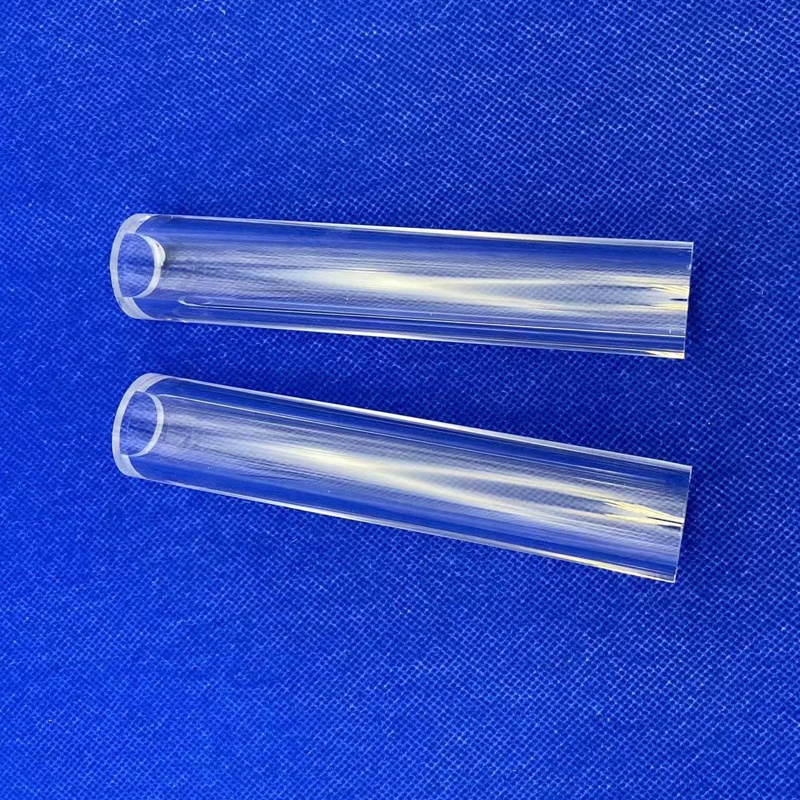
High-Purity Product Matrix

Precision Semiconductor Quartzware & Process Boats

Engineered to SEMI standards with thermal integrity up to 1300°C, zero-trace heavy metal contamination, and sub-millimeter slot tolerance for 100mm to 300mm wafer architectures.

≥99.99%
SiO₂ Chemical Purity
±0.02 mm
CNC Slot Pitch Precision
1100°C
Continuous Working Temp
14,271 m²
SGS Assessed Plant
Regional Application Architecture

High-Yield Deployment Across San Francisco & Greater Bay Area Fabs

The Northern California semiconductor ecosystem spans high-volume production lines, specialized MEMS micro-foundries, and academic nanocenters. Our OEM/ODM quartz wafer boats solve exact process bottlenecks across localized operational environments.

LPCVD & Atomic Layer Deposition (ALD)

Within fast-cycling Bay Area thin-film synthesis lines, quartz wafer boats experience corrosive chlorine, silane, and organometallic precursors. Our boats feature fire-polished, micro-crack-free slot cuts that eliminate particle sheds and chemical micro-retention.

  • No film flaking at high temperature gradients
  • Extended MTBF in Si₃N₄, Poly-Si, and HTO operations
  • Customized gas flow clearance slots to enhance film uniformity

Thermal Oxidation & Drive-In Diffusion

Operating continuously at 1050°C to 1200°C requires fused quartz with minimal trace alkali (Li, Na, K < 0.1 ppm) to prevent devitrification and wafer back-contamination. Our high-viscosity synthetic and natural fused quartz retain rigidity under high wafer-load payloads.

  • Sagging rate controlled below 0.05 mm across 500 thermal cycles
  • Sub-ppm sodium retention guaranteeing dielectric oxide gate purity
  • Configurable ladder, shell, and cantilever car designs

Compound Semi & Silicon Photonics

Silicon Valley's aggressive pivot toward optoelectronics, LiDAR, and optical computing engines necessitates non-standard wafer handling (InP, GaAs, SiC, and fused silica wafers). We produce custom-recessed boats preventing mechanical edge-chipping on fragile compound crystals.

  • Zero-rattle precision nest geometry for brittle III-V compounds
  • Custom chamfering for automated robot blade end-effectors
  • High optical transparency for optical in-situ wafer alignment
Semiconductor Macro Shifts

Bay Area Fab Upgrades: Navigating Sub-2nm Nodes & 3D Heterogeneous Packaging

The San Francisco Bay Area and greater Silicon Valley corridor remain the global epicenter of semiconductor IP and pilot-scale process pioneering. As fab engineers migrate toward Gate-All-Around (GAA) architectures, advanced 3D packaging, and silicon photonics interconnects, legacy quartzware faces severe thermal-stress boundaries.

Standard quartz components often fail to address the tightening requirement for slip-free high-temperature operations. In vertical and horizontal thermal diffusion, localized thermal expansion mismatch between silicon wafers and the quartz carrier generates micro-fractures and particle dislocation. Lovri Quartz addresses this with high-precision CNC slotting and strict polarization stress relief, ensuring that each wafer contact edge maintains an Ra < 0.4 µm finish, eliminating contact-induced crystallographic slip lines.

Furthermore, fab reshoring and CHIPS Act expansions throughout California emphasize domestic tool maintenance and rapid second-source supply chain verification. Procurement departments can no longer tolerate 16-to-24-week OEM lead times. By partnering directly with our primary production base in Lianyungang, Bay Area engineers obtain certified custom prototypes in under 14 days and full-batch shipments via expedited San Francisco International Airport (SFO) air-freight routing.

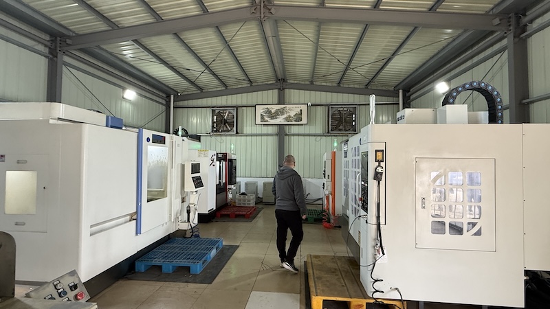
CNC Quartz Center Machining Wafer Boats
CNC 5-Axis Precision Slotted Wafer Boat Fabrication
Material Science Rigor

Chemical Purity vs. Hydroxyl Content (OH⁻): Balancing Thermal Longevity

In high-temperature semiconductor processing, optical transparency alone is insufficient. The longevity of a quartz wafer boat relies on controlling two opposing physical metrics: refractory viscosity (controlled by Hydroxyl OH⁻ concentration) and trace metal purity (Fe, Cu, Ni, Cr, Li, Na, K).

High OH⁻ concentration degrades quartz viscosity, causing horizontal boat rods to bow prematurely at temperatures exceeding 1050°C. Lovri Quartz executes proprietary vacuum dehydroxylation baking processes that reduce OH⁻ content to below 20 ppm on critical structural supports. For cold-wall wet etching or low-temperature ALD, we employ high-purity flame-fused silica providing near-zero bubble density and superior resistance to hot phosphoric acid and aggressive plasma species.

Every shipment bound for the Port of Oakland or SFO includes complete trace element batch assay sheets, confirming heavy metals remain within certified parts-per-billion (ppb) thresholds, securing your fab's yield budgets against unpredictable metallic drift.
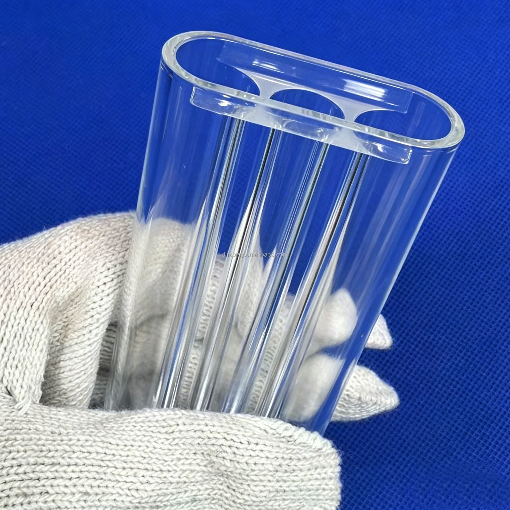
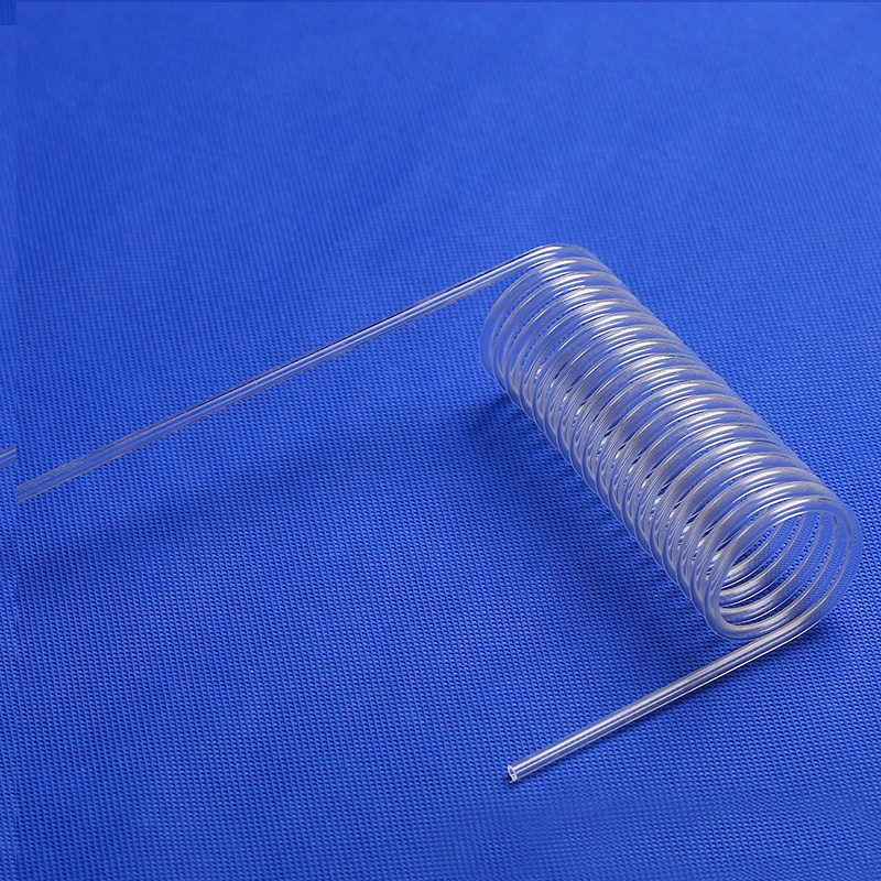
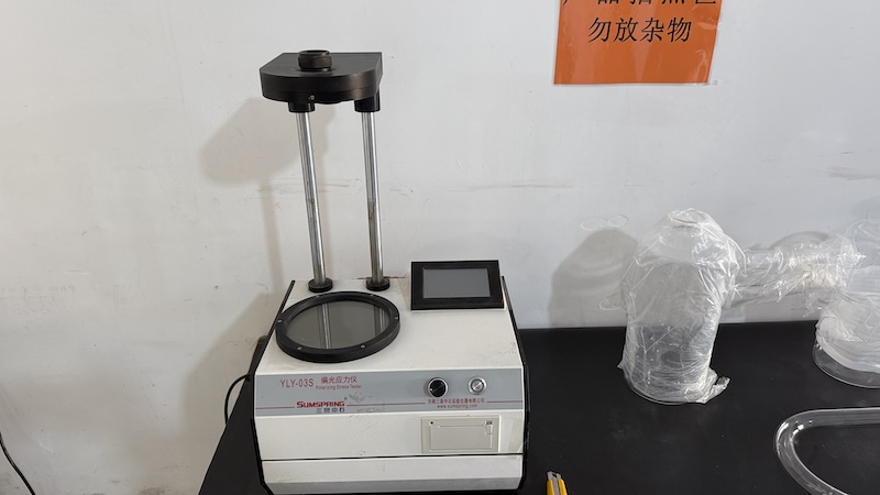
Polarization Stress Inspection of Quartz Components
In-House Polarization Stress Testing Verification
Physical / Chemical Property High-Purity Natural Quartz Synthetic Fused Silica (JGS1) Operational Fab Impact
SiO₂ Purity Level ≥ 99.99% (4N) ≥ 99.999% (5N) Prevents metallic dopant migration into active wafer channels
Density (20°C) 2.20 g/cm³ 2.201 g/cm³ Consistent structural payload-to-weight ratio
Thermal Expansion (20-300°C) 5.5 × 10⁻⁷ /°C 5.2 × 10⁻⁷ /°C Thermal shock endurance; prevents cracking during rapid furnace loading
Softening Point ≈ 1730 °C ≈ 1700 °C Prevents furnace sag during sustained 1200°C drive-in cycles
Hydroxyl (OH⁻) Content < 20 ppm (Dehydroxylated) < 1 ppm (Dry Grade) Extends mechanical stiffness; reduces devitrification speed
Slot Pitch Repeatability ±0.02 mm (CNC Ground) ±0.01 mm (CNC Optical) Seamless compatibility with ASML, Applied Materials, & TEL end-effectors
Direct Manufacturer Advantage

Why Tier-1 Semiconductor Buyers Choose Lovri Quartz

Located in Lianyungang, China's definitive quartz manufacturing hub, we operate an end-to-end integrated manufacturing facility assessed and verified onsite by SGS Group.

Primary Raw Material Control

We do not source third-party generic silica. We crush, pulverize, acid-pickle, and rescreen natural quartz lumps in our own facility, ensuring strict control over chemical purity before tube drawing begins.

  • No contamination from external supply disruptions
  • Guaranteed 99.99% minimum SiO₂ baseline across every melt
  • Dedicated acid pickling lines removing heavy transition ions

14,271 m² Verified Infrastructure

Our expansive industrial plant hosts dedicated CNC machining centers, automated high-temperature drawing towers, laser glass-cutting benches, cleanroom annealing lehrs, and clean packaging lines.

  • Assessed and verified onsite by SGS Group
  • Multi-axis CNC milling holding sub-micron profile tolerances
  • Class 10,000 clean assembly and acid pre-wash zones

100% Polarization Stress Inspection

Internal material stress is the leading cause of catastrophic explosion or collapse inside vacuum furnace tubes. We inspect 100% of finished boats and assemblies through optical polariscopes.

  • Complete residual stress neutralization via programmed annealing
  • Individual serialized QC documentation supplied with shipments
  • Dimensional verification against CAD / STEP specifications

Rapid Prototype to Production Scale

Silicon Valley start-ups and university labs need prototypes, while commercial foundries require high-volume repetitive production. We support both with custom MOQ starting at 1 piece.

  • Engineering review and DFM feedback within 24 hours
  • Fast-track 7-day turnaround for non-standard test geometries
  • Volume-tier economies of scale for established run-rates

Export-Certified Packaging Protocol

Transporting fragile quartz carriers across the Pacific demands engineering-grade packaging. We utilize customized foam molds, vacuum shrink sealing, and impact-isolated export crates.

  • Multi-layer high-density shock-absorbing EPE foam
  • Drop-tested wooden export crates compliance-stamped for US customs
  • Direct air-cargo tracking straight to your loading bay

Global Compliance & Traceability

All quartz products comply strictly with RoHS and REACH standards. We maintain full material heat traceability from silica mine intake to delivered semiconductor parts.

  • Certificate of Conformance (CoC) provided with each lot
  • RoHS compliant, non-hazardous fabrication workflow
  • Decades of trade experience with US customs and logistics
Procurement Knowledge Base

Frequently Asked Questions by San Francisco Procurement Teams

Detailed technical, logistics, and quality assurance answers compiled to streamline vendor verification and drawing onboarding for Northern California manufacturing plants.

How do you guarantee cleanroom-compatible cleanliness and zero contamination upon arrival in San Francisco?
All semiconductor-grade quartz wafer boats and tubes undergo ultrasonic acid cleaning (HF and high-purity DI water rinse) inside our controlled facility to dissolve loose surface particles and organic traces. Parts are dried with heated nitrogen, heat-sealed in double-layer anti-static cleanroom PE bags, and packed inside dust-free shock-isolated cartons. Upon receipt at your San Francisco Bay Area facility, components require only standard pre-diffusion clean cycles prior to furnace tube loading.
Can you manufacture replacement boats for obsolete or legacy furnace systems (e.g., Bruce, SVG, ASM, TEL)?
Yes. Many Bay Area semiconductor fabs maintain legacy 100mm, 150mm, and 200mm tooling where original equipment manufacturer parts are either end-of-life or cost-prohibitive. You can provide an engineering drawing (PDF, DWG, DXF, or STEP) or ship a physical worn or broken sample to our engineering department. Our reverse-engineering specialists will replicate slot pitches, cross-rod geometries, and handling ears with exact tolerances.
What is the typical lead time and shipping duration for deliveries to San Francisco, CA?
Custom prototypes typically take 7 to 12 working days to fabricate depending on slot intricacy and welding complexity. Standard production runs take 2 to 3 weeks. For urgent cleanroom replenishment, we ship via priority air freight (DHL, FedEx, or air cargo directly into San Francisco International Airport - SFO), delivering to your dock within 4 to 6 business days post-fabrication. For regular scheduled volume orders, consolidated sea freight via the Port of Oakland is available.
How do you verify slot pitch tolerance and perpendicularity on high-density wafer boats?
We utilize high-resolution non-contact optical coordinate measuring machines (CMM) and laser profile sensors to inspect each slot depth, width, and centerline pitch across the entire rod rack. Perpendicularity and slot parallelism are held within ±0.02 mm across lengths exceeding 400 mm, ensuring completely jam-free automation cycling with modern automated wafer transfer robots and vacuum end-effectors.
What is your policy regarding broken items damaged during overseas transit?
While our specialized custom-molded foam suspension and rigid plywood crate packaging results in a transit breakage rate below 0.1%, all export shipments are fully transit-insured. In the rare event of transit damage, notify us with photos within 48 hours of receipt. We immediately prioritize rush fabrication of replacement parts on our shop floor free of charge, minimizing your facility's furnace downtime.
Do you support custom wafer profiles, such as rectangular substrate carriers or ultra-thin wafer slots?
Yes. Beyond standard SEMI round wafers (100mm, 150mm, 200mm, 300mm), we frequently fabricate custom quartz boats for square photonic dies, thin glass microfluidic substrates down to 0.1mm thickness, MEMS cavity substrates, and oversized CVD furnace batches. Tell our engineering team your specific wafer diameter, thickness, and spacing needs for customized DFM advice.