Featured Quartz Substrates & Precision Components
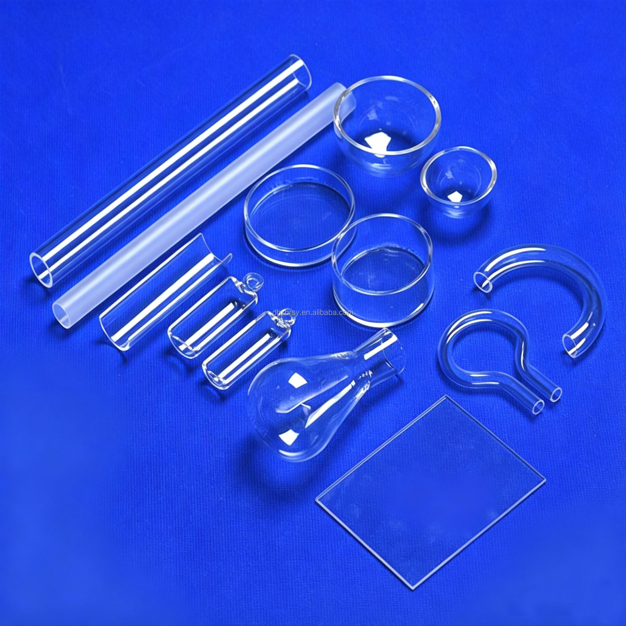
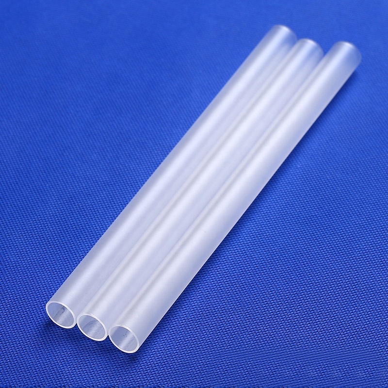
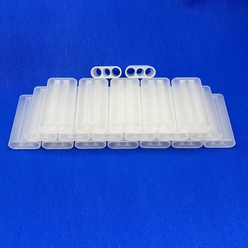
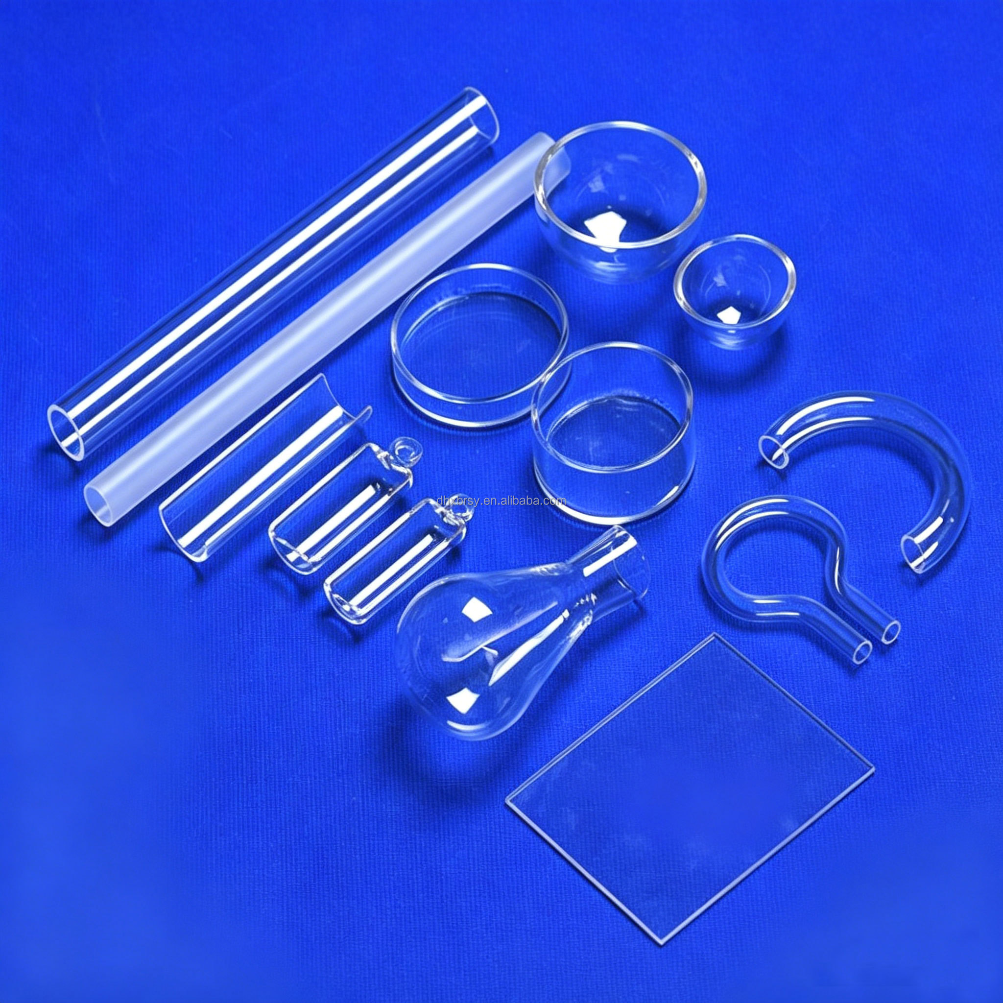
Direct factory supply of certified fused silica sheets, custom triple-bore flow channels, high-purity process apparatus, and optical wafers calibrated to rigid JIS semiconductor specifications.
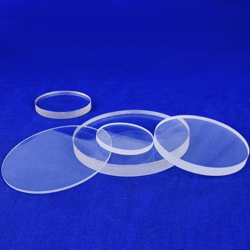
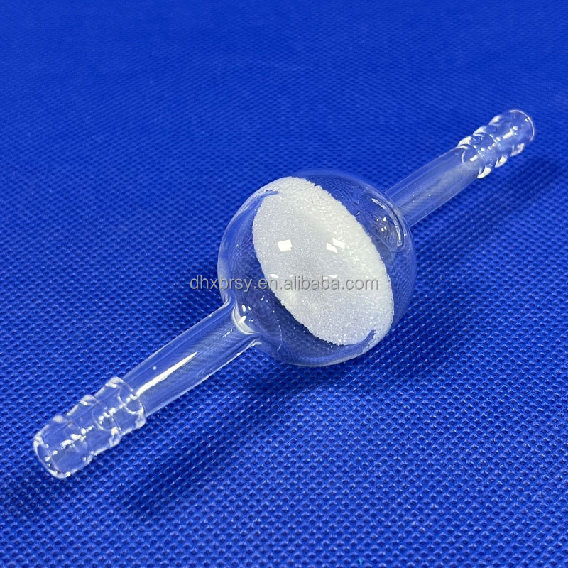
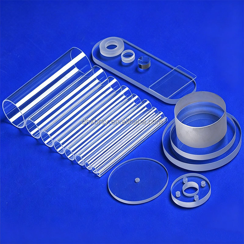
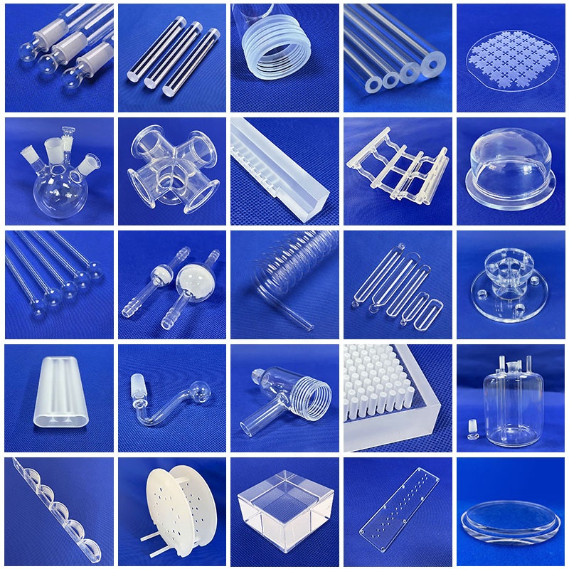
Evaluating High-Purity Quartz Substrates in Japan's Semiconductor Ecosystem
An authoritative engineering overview of structural purity, transmission bandwidths, and thermal stability requirements for Japanese precision manufacturing clusters.
As Japan accelerates investments across sub-2nm foundry initiatives in Hokkaido (Rapidus), expands power semiconductor manufacturing in Tohoku and Kansai, and consolidates advanced packaging lines throughout Kyushu ("Silicon Island"), the demand for optical-grade fused silica and fused quartz substrates has achieved historic highs. Precision components require physical stability, near-zero thermal expansion coefficients (5.5 × 10⁻⁷ /°C), and ultra-low levels of transition metal contamination (Fe, Cu, Ni < 0.1 ppm). Sourcing from an integrated source factory guarantees full control over raw material purification, drawing, polarization stress annealing, and final multi-axis CNC surface machining.
Unlike borosilicate glass, which softens at modest thermal regimes, transparent fused quartz manufactured via natural crystalline silica refinement maintains structural integrity at continuous working thresholds of 1100°C, with short-term heat peaks reaching 1300°C to 1400°C. In demanding photolithography stages, DUV exposure equipment, and plasma-enhanced chemical vapor deposition (PECVD), Lovri Quartz products deliver batch-to-batch consistency and total compliance with JIS standards and global RoHS environmental guidelines.
Primary Applications in the Japanese Industrial Landscape
From cleanrooms in Kumamoto to optical research laboratories in Tsukuba, our substrates power mission-critical hardware.
Semiconductor Wafer Jigs & Photomasks
Widely integrated across Japanese fab tooling lines in Kyushu and Hiroshima. Fused silica substrates serve as stable carrier wafers, photomask blanks, and high-temperature furnace boats that resist heavy chemical attack during RCA clean, hot phosphoric acid strip, and fluorine plasma etching.
MEMS & Microfluidic Devices
Japanese biomedical apparatus developers rely on our double-side polished (DSP) quartz plates with Ra < 0.3 nm. The optical transparency from deep UV to near-infrared eliminates auto-fluorescence background interference during high-throughput genomic screening and lab-on-a-chip laser interrogation.
Industrial Laser & LiDAR Window Systems
Deployed across Nagoya and Kanto automotive hubs. Fused quartz substrates endure thermal shock in fiber laser cutting head windows, laser beam delivery nozzles, and exterior-grade LiDAR sensor shields requiring superior mechanical strength against debris abrasion and rain erosion.
Advanced Photovoltaic & Green Energy
Japanese solar research facilities utilize high-transmittance quartz furnace tubes and quartz boats for TOPCon and next-generation perovskite-silicon tandem cell crystallization, ensuring zero metallic atom outgassing during long-duration thermal annealing runs.
Optical Quartz Grades: JGS1 vs. JGS2 vs. JGS3
Selecting the correct quartz raw material specification to balance optical transmission windows, hydroxyl (OH⁻) content, and cost.
| Characteristic / Parameter | JGS1 (Synthetic Fused Silica) | JGS2 (Optical Fused Quartz) | JGS3 (Electrically Fused Quartz) |
|---|---|---|---|
| Raw Material Origin | High-purity SiCl₄ chemical vapor synthesis | Refined natural quartz crystals (flame fusion) | High-purity quartz sand (electric vacuum melt) |
| Transmission Spectrum Range | 185 nm – 2500 nm (Deep UV to Vis) | 220 nm – 2500 nm (Standard Optical) | 260 nm – 3500 nm (Infrared Enhanced) |
| Hydroxyl (OH⁻) Content | High (typically ~1000–1200 ppm) | Moderate (~150–200 ppm) | Extremely Low (< 5 ppm) |
| Bubble / Inclusion Class (ISO 10110) | 0/0 (Virtually bubble-free) | Class 1–2 (Minor micro-bubbles allowed) | Class 2–3 (Process furnace grade) |
| Refractive Index (nd at 589.3 nm) | 1.4585 | 1.4585 | 1.4585 |
| Key Japanese Sourcing Application | ArF/KrF steppers, DUV laser optics, UV curing | Spectrophotometer cells, viewports, jigs | Thermal infrared emitters, CVD process chambers |
Localized Sourcing Trends Driving Japanese Procurement Teams
How Japanese tier-1 device fabricators and machinery exporters navigate raw material quality, resilience, and ESG compliance.
1. Stringent 4M Change Notification
Japanese QA protocols mandate rigorous control over Man, Machine, Material, and Method (4M). Sourcing managers reject unannounced shifts in raw sand suppliers or CNC tooling lines. Lovri Quartz provides signed 4M freeze agreements, batch chemical analysis certificates, and stable lot tracking.
2. Ultra-Flatness & TTV Requirements
With wafer packaging evolving toward 2.5D/3D chiplet stacking and temporary glass bonding, Total Thickness Variation (TTV) < 1 µm and bow/warp < 5 µm are now strict engineering prerequisites across Kanto equipment makers. Our multi-stage double-side chemical-mechanical planarization (CMP) fulfills this requirement.
3. Supply Resilience & Direct Factory Auditing
To hedge against single-region supply blockades and trading house markups, Japanese purchasing directors increasingly secure direct relationships with verified source factories. Lovri Quartz's on-site SGS assessment, full transparency, and short air/sea freight routing to Tokyo, Yokohama, and Hakata ensure unmatched continuity.
Why Engineering Teams Choose Lovri Quartz
Vertical integration from silica lump selection to final polarization stress validation in our certified 14,271 m² manufacturing campus.
Fully Integrated Mineral Refinement
We do not depend on untracked third-party glass blanks. Located in Lianyungang, China's quartz heartland, we operate in-house lump crushing, pulverizing, rescreening, and multi-stage chemical acid pickling to yield 99.99% SiO₂ baseline purity before thermal drawing begins.
5-Axis CNC Precision Machining
Our CNC workshops handle intricate CAD drawings (STEP, DWG, DXF, PDF). From micron-accurate slotting for semiconductor wafer boats to blind-hole drilling in 96-well microplates and fire-polished edges, every tolerance is metrology-checked with coordinate measuring machines (CMM).
Polarization Stress & Bubble Testing
Residual internal stress causes sudden quartz shattering during rapid thermal cycling in semiconductor reactors. Every annealed component in our factory undergoes non-destructive polarization stress testing, laser interferometry, and spectrophotometer verification prior to shipment.
Frequently Asked Questions by Japanese Procurement Teams
Clear, direct technical answers addressing customs, surface finishes, packaging integrity, and quality documentation.
Can you provide inspection certificates complying with Japanese Industrial Standards (JIS)?
Yes. We regularly supply detailed Mill Test Certificates (MTC), dimensional CMM reports, spectrophotometric transmittance graphs (UV-Vis-NIR), and polarization stress birefringence measurements that correspond with JIS R 3202 and relevant semiconductor equipment guidelines.
How do you prevent fragile quartz substrate breakage during transit to Japan?
We implement a 3-layer export safety packaging system: individual static-free cleanroom wrapping, multi-axis custom-cut high-density EPE foam cradles, and heat-treated, fumigated plywood export cases with corner impact braces and external tip-and-tell shock indicator sensors.
What is your minimum order quantity (MOQ) for custom-engineered prototypes?
To support Japanese R&D centers, university research labs (such as Tokyo University, Kyoto University, Tohoku University), and fab prototyping cycles, we accept prototype orders starting from 1 to 5 pieces for custom drawings before committing to mass volume production runs.
What surface roughness (Ra) and flatness parameters can your polishing line achieve?
Our CMP optical polishing lines consistently deliver surface roughness Ra < 0.3 nm (sub-nanometer super-polish), surface figure error / flatness < λ/4 at 632.8 nm, and scratch-dig specifications complying with US MIL-PRF-13830B 20/10 or ISO 10110 standards.
How do you handle hazardous material compliance (RoHS & REACH)?
All fused quartz products are 100% inorganic synthetic or natural high-purity SiO₂. Full third-party RoHS and REACH test reports from SGS Group are available for every delivery batch, validating non-detectable levels of lead, cadmium, mercury, and halogen compounds.
What shipping terms and lead times apply for air freight to Narita, Haneda, or Kansai?
Standard prototype lead time is 7–14 working days after final CAD confirmation. We offer FCA, FOB, CIF, or DDP terms. Utilizing direct air logistics from Shanghai (PVG) or Qingdao (TAO) to Tokyo or Osaka, in-transit cargo time averages only 48 to 72 hours.
Connect Directly with Our Quartz Engineering Team
Send your 2D/3D CAD drawings (STEP, DWG, PDF) or application parameters. Our optical and semiconductor quartz specialists will review manufacturability, specify optimal material grades, and supply a competitive direct factory quote within 24 hours.