Precision Tube
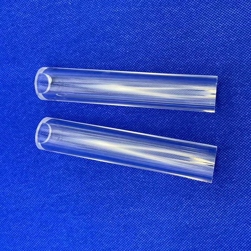
Clear Fused Silica Quartz Glass Tube
High-precision bending, thermal welding, cutting tolerances for ozone units and industrial far-infrared heating assemblies.
Product DetailsDirect manufacturing of high-purity optical flats, reaction tubes, and semiconductor-grade wafer carriers meeting stringent European microelectronic and laboratory criteria.
High-precision bending, thermal welding, cutting tolerances for ozone units and industrial far-infrared heating assemblies.
Product Details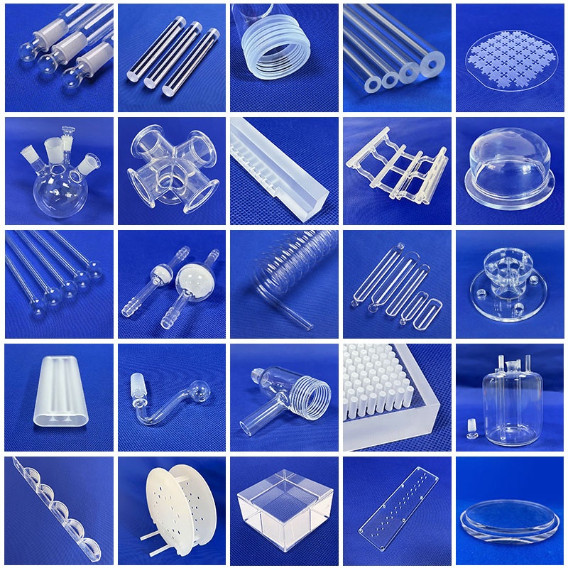
Double-sided optical polishing with white rim finishing. Delivers premium transmission across UV to near-infrared spectrums.
Product Details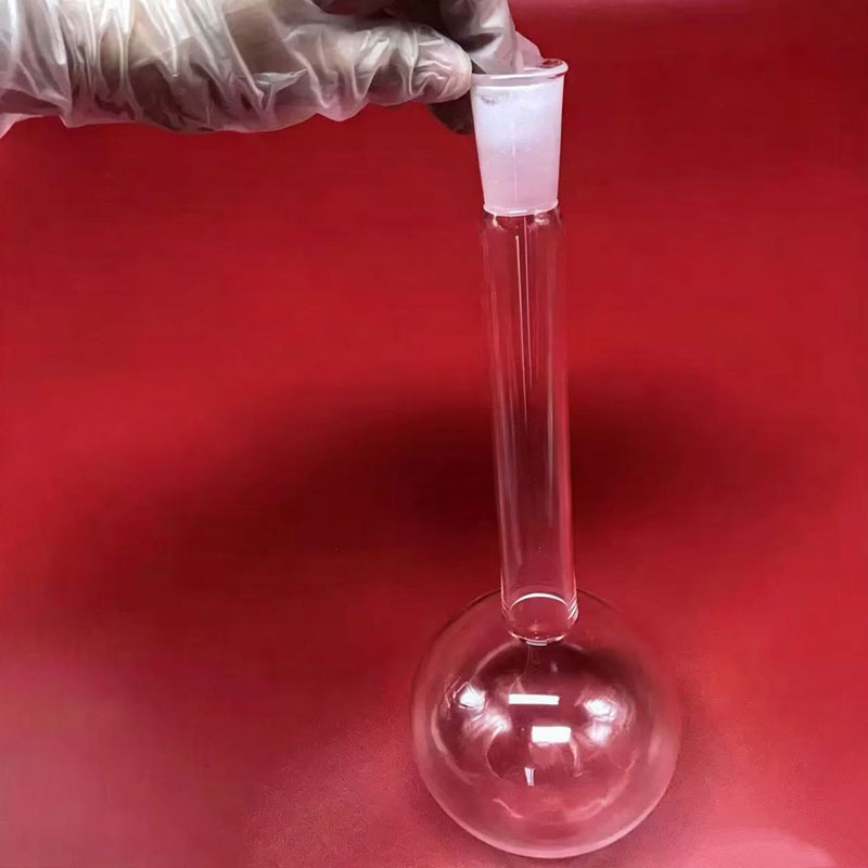
Continuous resistance up to 1200 °C. Inert to aggressive reagents, RoHS certified for critical biochemistry labs.
Product Details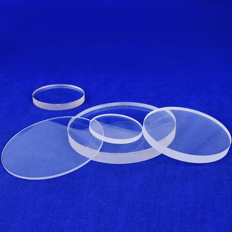
200 mesh grade surface polishing, ultra-flatness, designed specifically for industrial laser windows and wafer substrates.
Product Details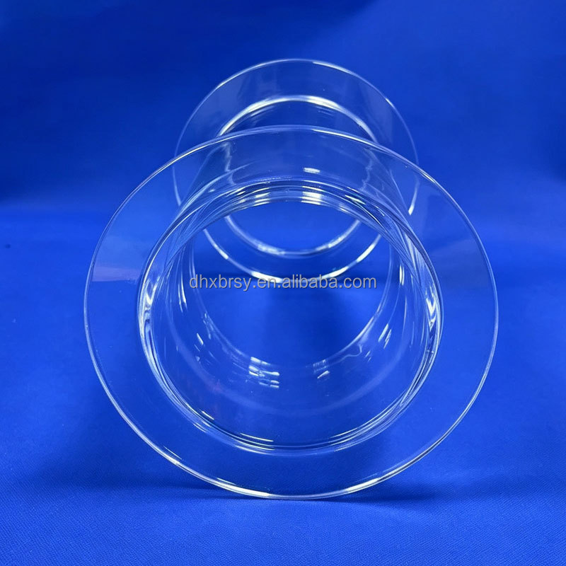
High-vacuum sealing flanges, uniform wall thickness, optimized for semiconductor CVD, ALD, and oxidation chambers.
Product Details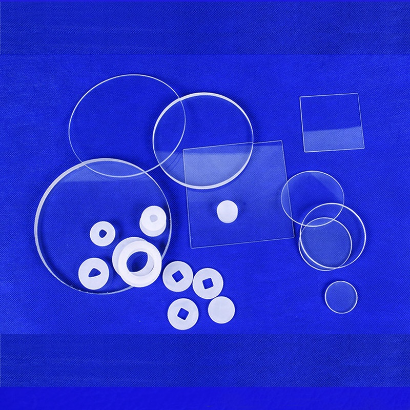
Deep-UV transparent (185–2500 nm), strictly annealed to remove internal birefringence for laser beam transmission.
Product Details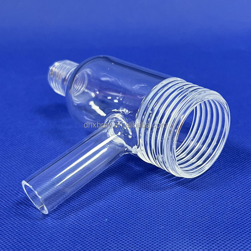
CNC micro-machined threaded interfaces for high-temperature fluidic and gas connections without thermal leakage.
Product Details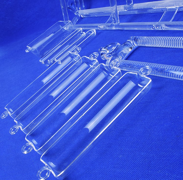
Engineered slot tolerances for 2-inch to 8-inch wafers. High mechanical integrity for high-temperature diffusion furnaces.
Product DetailsWhile the Principality of Monaco is globally renowned for luxury, its proximity to Sophia Antipolis and its own advanced marine research, precision instruments, and high-tech clean labs create demanding requirements for high-purity fused silica.
Scientific entities such as the Scientific Centre of Monaco (CSM) and the IAEA Marine Environment Laboratories rely on JGS1 deep-UV transparent fused silica windows. These wafers permit exact, uncorrupted spectrophotometric measurements of heavy metals, oceanic acidification markers, and radiometric isotopes across UV-visible spectra.
Connected closely with the Côte d'Azur microelectronics corridor, Monte Carlo engineering firms source custom 2-inch to 8-inch fused silica wafers. Due to fused silica's negligible dielectric loss and extreme electrical insulation, these wafers serve as base substrates for surface acoustic wave (SAW) filters, high-frequency photonics, and planar lightwave circuits.
Monaco's premier cosmetic and dermatological treatment centers deploy high-energy solid-state Nd:YAG and Alexandrite lasers. Our double-side polished fused quartz plates and triple-bore flow cooling tubes withstand intense optical power densities exceeding 10 J/cm² without developing laser-induced damage or solarization effects.
A rigorous metallurgical comparison designed to guide laboratory directors, optical physicists, and technical buyers toward the correct substrate selection.
| Physical / Chemical Property | JGS1 Synthetic Silica | JGS2 Flame-Fused Quartz | JGS3 Electrically-Fused Quartz |
|---|---|---|---|
| Optical Transmission Range | 185 nm – 2500 nm (Deep UV) | 220 nm – 2500 nm (Standard Optical) | 260 nm – 3500 nm (High IR) |
| SiO₂ Purity Grade | ≥ 99.999% | ≥ 99.99% | ≥ 99.95% |
| Coefficient of Thermal Expansion (CTE) | 5.5 × 10⁻⁷ /°C (20°C–320°C) | 5.5 × 10⁻⁷ /°C (20°C–320°C) | 5.4 × 10⁻⁷ /°C (20°C–320°C) |
| Surface Roughness (Polished Wafer) | Ra < 0.3 nm (Super-polished) | Ra < 0.5 nm (Optical standard) | Ra < 0.8 nm (Commercial flat) |
| Total Hydroxyl (OH⁻) Content | < 1200 ppm | < 150 – 200 ppm | < 5 ppm (Water-free IR) |
| Maximum Strain Point | 1070 °C | 1120 °C | 1120 °C |
How Mediterranean advanced manufacturing networks are optimizing supply chain reliability and cost-to-performance efficiency via direct factory partnerships in China.
Deep-ultraviolet sanitization and photolithography research require substrates devoid of localized bubbling and inclusions. Monégasque engineering groups are shifting away from commercial borosilicate towards class-0 bubble-free synthetic silica wafers, eliminating micro-lens light scattering.
European distributors frequently add massive markups (up to 300%) on basic optical discs. Direct procurement from Lianyungang manufacturing clusters allows R&D hubs in the Monte Carlo region to access certified substrates at tier-one production costs with comprehensive SGS chemical assay documentation.
Emerging applications in MEMS pressure transducers and photonic integrated circuits demand substrates with thicknesses as fine as 0.1 mm to 0.3 mm. Direct chemical-mechanical polishing (CMP) by specialized Chinese exporters meets total thickness variation (TTV) targets below 2 microns.
Combining primary mineral processing, automated drawing towers, and five-axis CNC machining under one SGS-certified roof in Lianyungang, Jiangsu.
We process natural raw silica lump to high-purity sand in-house through calcination, crushing, screening, and intense acid pickling. This guarantees baseline SiO₂ content of 99.99% without third-party feedstock variability.
Our machine shop handles multi-bore drilling, micro-fluidic slotting, optical edge polishing, and high-precision threading to DWG, STEP, or PDF prints with dimensional tolerances held to ±0.02 mm.
Every single annealed glass batch passes through optical polariscope testing to identify and eliminate internal thermal stress fields. This prevents thermal shock failures when operating at temperatures up to 1300 °C.
Wafers and precision tubes are vacuum-packaged, cushioned in multi-density polyethylene foam, and secured inside reinforced wooden crates rated for door-to-door express and air transit to the French Riviera.
Clear, direct answers regarding customs clearance, European standards compliance, and order customization.
Consult our factory engineering department directly. Receive an itemized technical evaluation, lead-time estimate, and transparent factory-direct quote within 24 hours.
Get Catalog