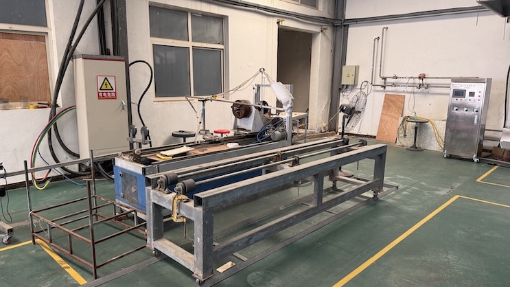
STEP 01
Raw Material Cutting
Selected high-grade quartz crystals undergo mechanical sizing and grading.
Engineered to eliminate micro-particulate shed, withstand aggressive halogenated chemistries at >1150 °C, and maintain tight vacuum-seal tolerances for LPCVD, PECVD, and ALD batch reactors.
Fab-Grade Verification. Audited for Global Semiconductor Fabs.
 Onsite Assessed by SGS
 Verified Supplier
 CE Compliant
Exporting critical CVD process components directly to cleanrooms in


Chemical Vapor Deposition processes demand reaction containment cylinders that endure extreme plasma flux, corrosive reactive gas precursors, and sharp thermal ramp rates without particle shedding or chamber warping.
In thermal Low-Pressure Chemical Vapor Deposition (LPCVD) and Plasma-Enhanced Chemical Vapor Deposition (PECVD), the quartz cylinder serves both as a structural vacuum boundary and an isothermal radiative envelope. Achieving consistent deposition layer thickness on 200 mm and 300 mm silicon wafers requires extreme concentricity and wall-thickness consistency across lengths often exceeding 2,000 mm.
Variations in wall thickness greater than 0.2 mm induce localized hot spots, triggering non-uniform boundary layer stagnation and uneven chemical decomposition of silane (SiH4), dichlorosilane (DCS), or metallo-organic precursors. Lovri Quartz Products Co., Ltd. addresses this through computer-automated drawing and precision mechanical sizing to maintain wall concentricity within ±0.03 mm.
Get CatalogDevitrification—the phase transformation of amorphous fused silica into crystalline cristobalite—is the primary mechanical failure mechanism in semiconductor quartz cylinders operating above 1,000 °C. This transformation causes micro-cracking due to a 5% volume contraction during thermal cycling, which releases microscopic silica particulate into the fab gas stream and ruins die yields.
Because devitrification is kinetically catalyzed by trace alkali metals (specifically Sodium, Potassium, and Lithium), standard industrial quartz glass is unacceptable. Lovri Quartz integrates intensive hot-acid pickling in our clean production cells to suppress surface alkali impurities below 0.1 ppm, preventing nucleation sites and dramatically prolonging chamber operational lifetimes.
Request Engineering AuditReview our standard fab-grade chamber liner and process cylinder classifications built to SEMI standard specifications.
| Configuration Type | Operating Process | Working Temp | Material Grade | Critical Geometrical Features |
|---|---|---|---|---|
| Vertical Double-Wall LPCVD Cylinder | Silicon Nitride (Si3N4), Poly-Si Deposition | 800 °C – 1150 °C | Synthetic / Electric-Fused Fused Silica (>99.995%) | Integrated dual cooling jackets, ground vacuum sealing flanges, laser-machined exhaust ports. |
| Horizontal Diffusion/CVD Process Cylinder | Atmospheric Oxidation, TEOS Oxide Deposition | 950 °C – 1250 °C | High-Purity Natural Quartz (>99.99%) | Smooth bellmouth or domed sealed end, welded thermocouple wells, heavy-duty quartz support rings. |
| PECVD Chamber Plasma Liner Cylinder | Dielectric Barrier, SiON, Low-k Films | 200 °C – 550 °C | Opaque / Clear Composite Fused Silica | Micro-bead blasted interior (Ra 2.5–3.5 µm) for optimal film adhesion to reduce chamber flaking. |
| Atomic Layer Deposition (ALD) Quartz Cylinder | High-k Gate Oxides (Al2O3, HfO2), Ultra-thin films | 150 °C – 450 °C | Optical Ultra-Smooth JGS1 Grade Fused Silica | Precision CNC manifold connections, helium leak-tested to < 1 x 10^-9 mbar·L/s. |
As the semiconductor manufacturing roadmap moves toward Gate-All-Around (GAA) architectures, advanced 3D-NAND stack heights exceeding 300 layers, and heterogeneous chiplet packaging, CVD quartz cylinders face rigorous operational challenges.
As legacy 150mm and 200mm fabrication nodes convert or expand to 300mm wafer operations, the mechanical demands on CVD quartz cylinders grow exponentially. Cylinders spanning outside diameters of 350 mm to 480 mm with lengths exceeding 2,200 mm experience substantial gravitational sag and creep deformation under cyclic thermal loading. Fab procurement managers are standardizing on quartzware verified by polarization stress profiling to guarantee residual stress lower than 1.5 MPa along weld seams.
Next-generation batch atomic layer deposition systems utilize aggressive fluorine- and chlorine-based radical cleanings (NF3, ClF3). Unprotected quartz walls undergo etching, creating pinholes and particle generation. The industry trend leans heavily toward specialized inner-wall treatments, precision flame polishing, and micro-engineered surface roughness that balances precursor residence times with high-adhesion film resistance to stop flaking.
Global trade volatility and high-purity silica sand raw material shortages have elevated supply chain predictability to a C-level priority. Semiconductor OEMs and tiered chipmakers are actively bypassing brokers to contract directly with integrated quartz manufacturers. Facilities that control raw quartz processing, drawing, high-temperature annealing, and cleanroom CNC machining in-house guarantee uninterrupted batch deliveries and 100% material traceability.
Manual measuring calipers and standard bubble inspection no longer satisfy ISO Class 3/4 cleanroom entry criteria. Procurement protocols now mandate full Coordinate Measuring Machine (CMM) digital verification, laser interferometer roundness profiling, and multi-stage cleanroom ultrasonic degassing prior to Class 100 vacuum packaging.
Lovri Quartz Products Co., Ltd. operates a premier fused quartz manufacturing complex situated in Lianyungang, Jiangsu — China’s premier industrial silicon cluster. Our integrated manufacturing infrastructure encompasses 14,271 m² of production and specialized cleanroom testing space.
By keeping raw material pulverization, multi-stage chemical acid pickling, automated horizontal tube drawing, high-temperature annealing furnaces, and multi-axis CNC machining under one roof, we eliminate intermediate supply interruptions and ensure total batch traceability for mission-critical semiconductor components.
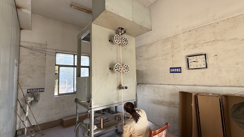
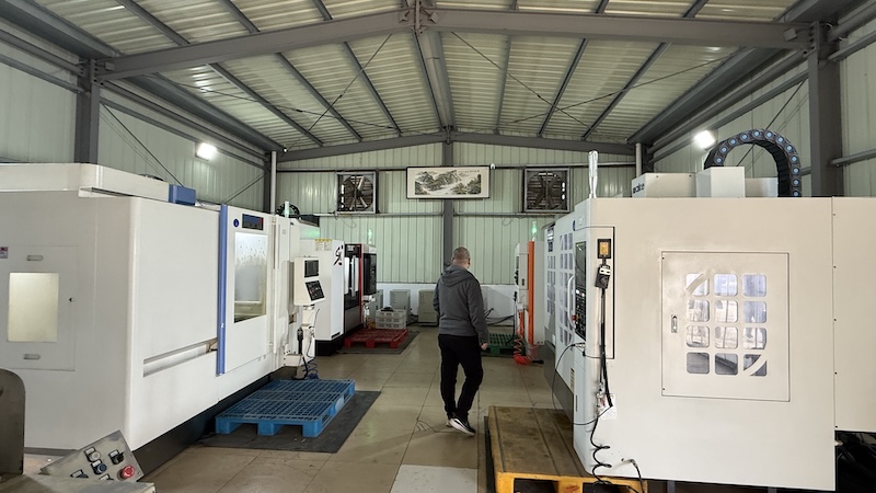
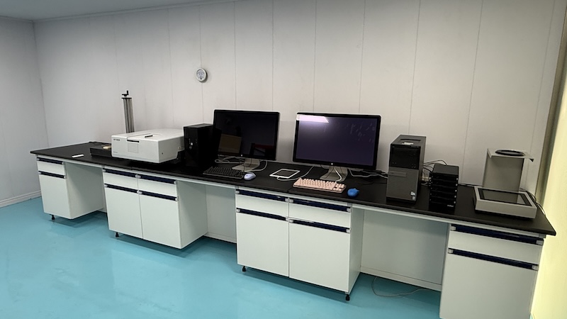
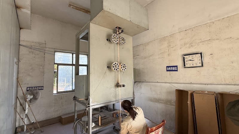
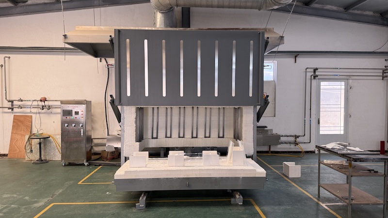
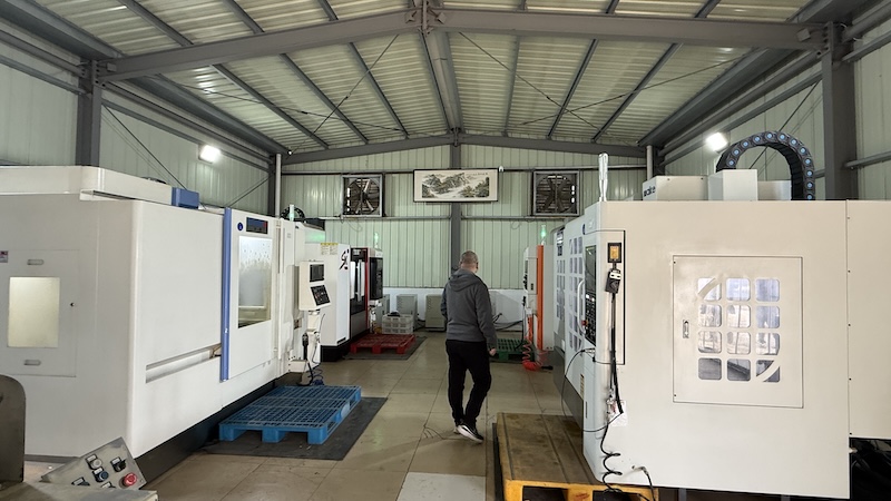
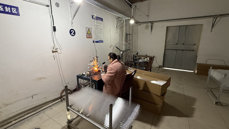
From mineral sand preparation to final cleanroom packaging, discover how Lovri Quartz Products Co., Ltd. controls purity, stress, and geometry at every step.
Selected high-grade quartz crystals undergo mechanical sizing and grading.
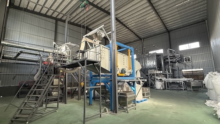
Crystalline raw materials are pulverized into uniform micro-granules.
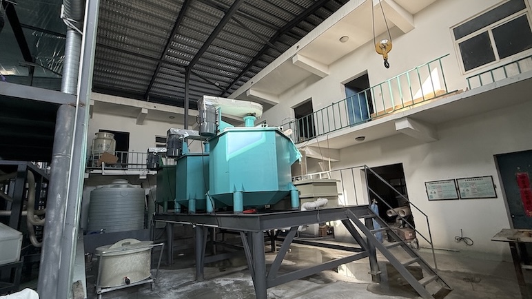
Granular classification ensures strict mesh consistency prior to smelting.
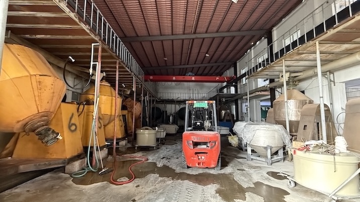
Deep multi-acid leaching extracts metallic traces to attain >99.995% SiO2.
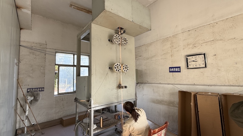
High-temperature drawing produces large-diameter quartz cylinder cylinders.
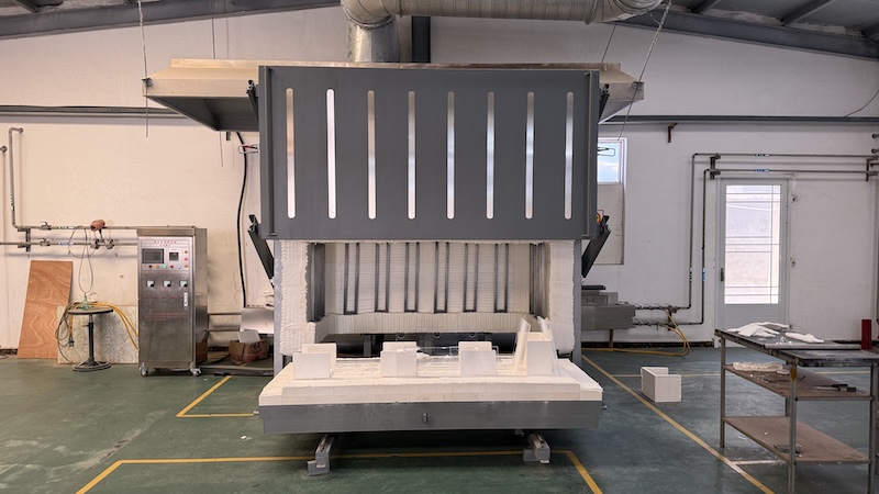
Programmed cooling profiles completely relieve thermo-mechanical stresses.
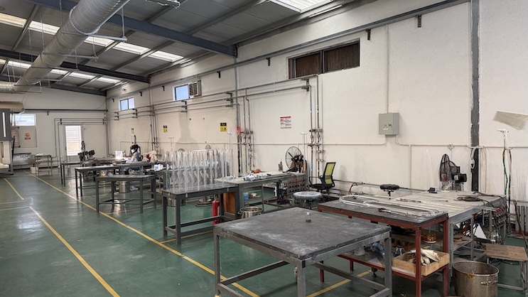
Precision thermal shaping of bellmouths, domed tops, and bottom flanges.
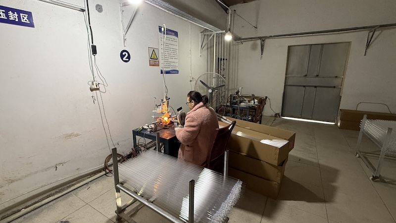
Torch lathe welding of gas injectors, flanges, and quartz support collars.
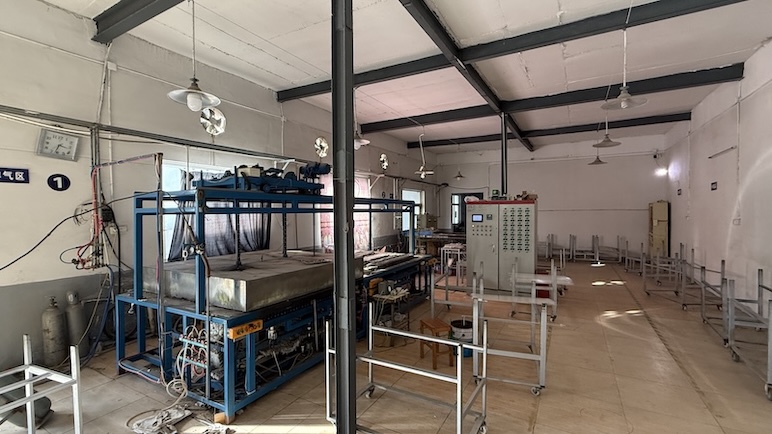
Thermal vacuum baking out-gases hydroxyl groups (OH) and volatile species.
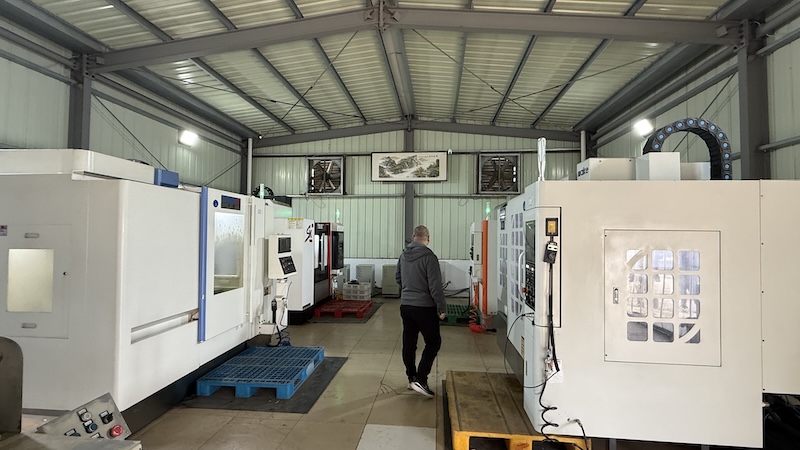
Diamond grinding of sealing faces, gas slots, and bolt holes down to ±0.03 mm.
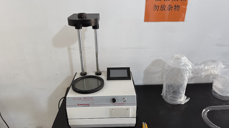
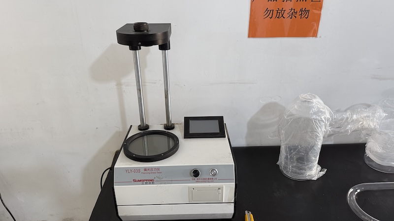
Laser concentricity checks, CMM metrology, and polarimeter stress verification.
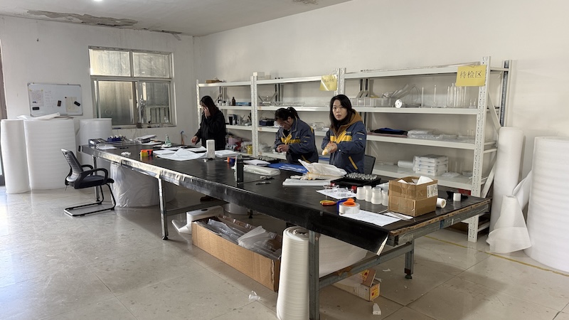
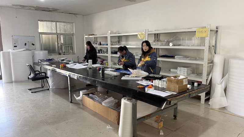
Multi-layer shock absorbing cleanroom pack in reinforced export wooden cases.
Why global semiconductor device fabricators, etching equipment builders, and research centers trust Lovri Quartz Products Co., Ltd.
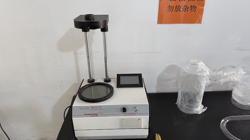
Thermal-gradient-induced mechanical failure in CVD chambers causes disastrous downtime. Lovri Quartz subjects every single batch of semiconductor CVD quartz cylinders to strict qualitative and quantitative polarization stress analysis.
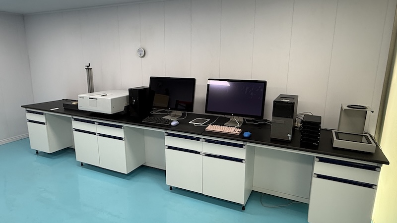
Our analytical metrology laboratory verifies chemical element concentrations at the parts-per-billion level using Inductively Coupled Plasma Mass Spectrometry (ICP-MS).
Hermetic O-ring and metal-gasket vacuum joints require flawless geometric precision. Our 5-axis ultrasonic and diamond grinding facilities achieve semiconductor-grade dimensional fidelity.
Large-format quartz cylinders are susceptible to micro-fractures during multi-modal international freight. We design custom nested packaging engineered specifically for long-distance transport.
Production facility and capacity confirmed
International corporate audit accreditation
Conformity to international safety criteria
Substance-controlled semiconductor clean materials
Fused silica reaction cylinders perform essential isolation, thermal conduction, and plasma confinement roles across advanced wafer-fabrication unit operations.
Containment of high-temperature pyrolysis in poly-silicon, silicon nitride, and doped oxide processes.
Internal reactor liners safeguarding chamber walls from corrosive RF plasma attack and unwanted film build-up.
Ultra-smooth cylinders facilitating rapid precursor purge cycles with zero gas wall adsorption.
Engineered flow cylinders for GaN and GaAs compound semiconductor crystal growth reactors.
High infrared-transmittance process enclosures supporting fast thermal ramping up to 1200 °C.
Heavy-duty process tubes ensuring phosphorus and boron dopant uniformity in TOPCon and HJT solar cells.
Precision-ground fused silica confinement rings protecting wafer edges during chlorine/fluorine plasma etching.
Tailored quartz vessels, flow reactors, and observation cylinders designed to custom laboratory prints.
Select a specific category below to view technical attributes or browse our full inventory of standard and custom fabrications.
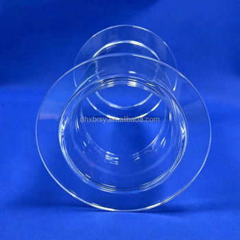
Transparent fused silica · Semiconductor CVD chambers · Tight flatness
View Series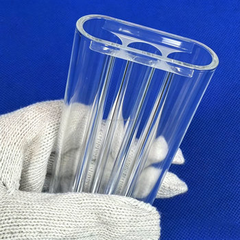
High-temperature fused silica · Annealing & diffusion nodes · 1250 °C
View Series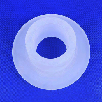
Thermal crack-resistant · CNC bolt patterns · High vacuum mating
View Series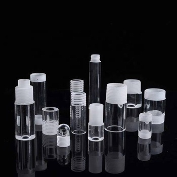
Engineered geometry · Hand torch and CNC fusion · Strict annealing
View Series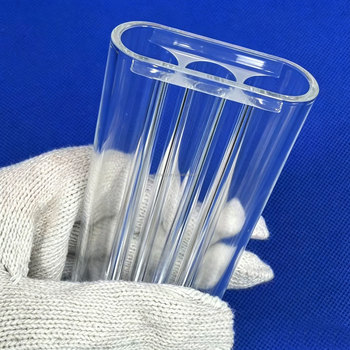
Milled & polished · ±0.03 mm tolerances · Semiconductor jigs
View Series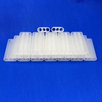
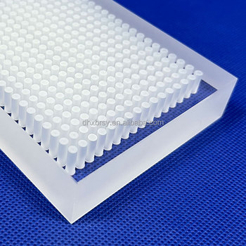
Drilled optical wells · Chemical resistance · Zero cross-talk
View Series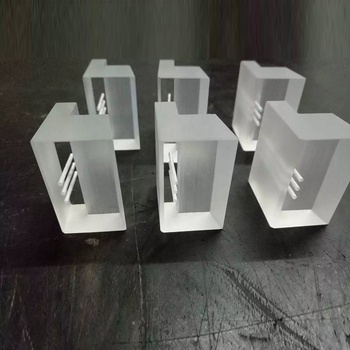
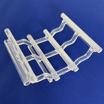
Accurate slot pitch · 99.995% purity · Minimal wafer shadow
View Series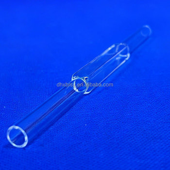
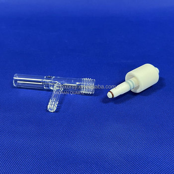
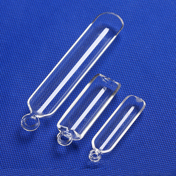
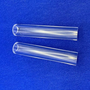
Tight outer/inner diameter tolerances · 99.99% SiO2 · Custom cut
View Series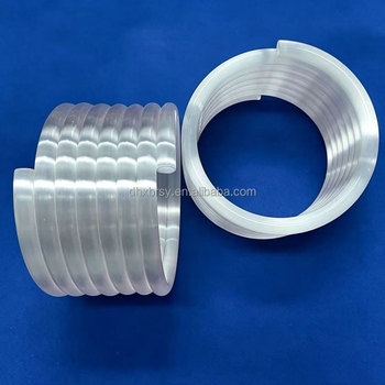
Infrared reflection · Dense thermal isolation · CVD heating jackets
View Series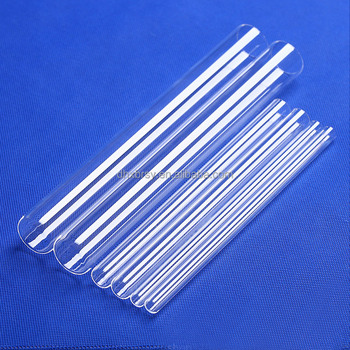
Short-term resistance to 1300 °C · Fire polished closed domed end
View Series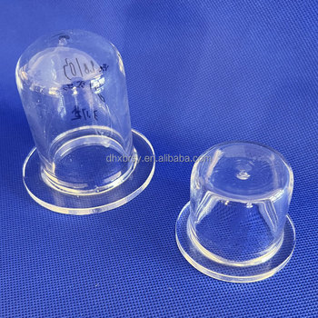
High transmission · Thermal shock resistant · Large OD drawing
View Series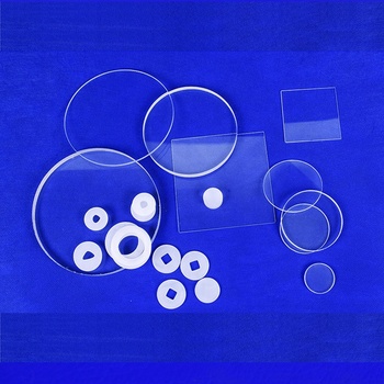
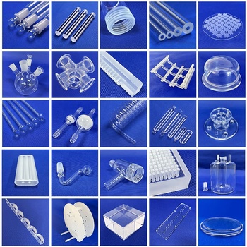
Corrosion-resistant · Ra < 0.5 nm polish · Semiconductor masks
View Series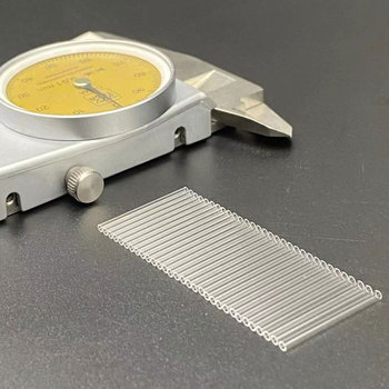
0.1 mm to 0.5 mm · Precision thickness · High dielectric strength
View Series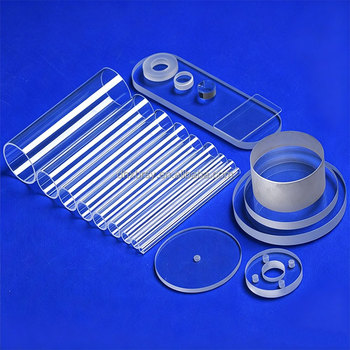
JGS1/JGS2 synthetic · Pyrometer observation window · High vacuum
View Series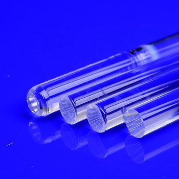
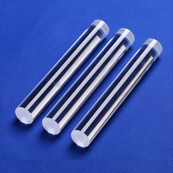
Purity >99.99% · Structural support for CVD quartz cassettes
View Series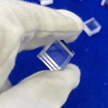
Precision polished faces · Fab photolithography & optical links
View Series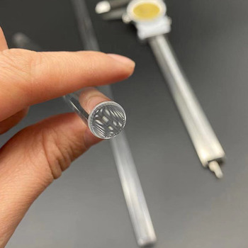
Semi-circular, square, oval profiles · Custom furnace track rails
View SeriesReview critical thermodynamic constants, trace metallic tolerance thresholds, and common technical answers addressed by Lovri Quartz technical specialists.
| SiO₂ Chemical Purity | ≥ 99.995% (Synthetic grades up to 99.999%) |
|---|---|
| Density | 2.20 g/cm³ |
| Thermal Expansion Coefficient (20–300 °C) | 5.5 × 10⁻⁷ /K (Outstanding thermal shock resistance) |
| Softening Point | ≈ 1730 °C |
| Annealing Temperature (Stress Relief) | ≈ 1215 °C |
| Continuous Operating Temperature | Up to 1150 °C (1250 °C for low OH electrically fused) |
| Dielectric Constant (at 1 MHz) | 3.75 |
| Permissible Residual Stress | < 1.5 MPa (Polariscope validated) |
| Helium Vacuum Leak Rate | < 1.0 × 10⁻⁹ mbar·L/s (With CNC ground O-ring seal) |
| Element | Max Limit | Element | Max Limit |
|---|---|---|---|
| Al (Aluminum) | < 14.0 ppm | Fe (Iron) | < 0.15 ppm |
| Na (Sodium) | < 0.10 ppm | K (Potassium) | < 0.10 ppm |
| Li (Lithium) | < 0.10 ppm | Ca (Calcium) | < 0.40 ppm |
| Cu (Copper) | < 0.05 ppm | Cr (Chromium) | < 0.05 ppm |
ICP-MS and polarization test certificates are issued per manufacturing batch by Lovri Quartz Products Co., Ltd. custom testing laboratory.
Submit your part drawings, operating process parameters, temperature specifications, and batch requirements. The Lovri Quartz engineering team provides comprehensive manufacturability reviews and firm quotes within 24 hours.