Featured CE & RoHS Certified Fused Silica Components
Engineered to strict dimensional tolerances (±0.02 mm) and subjected to comprehensive polarization stress analysis, each component is calibrated for critical thermal and chemical duty.
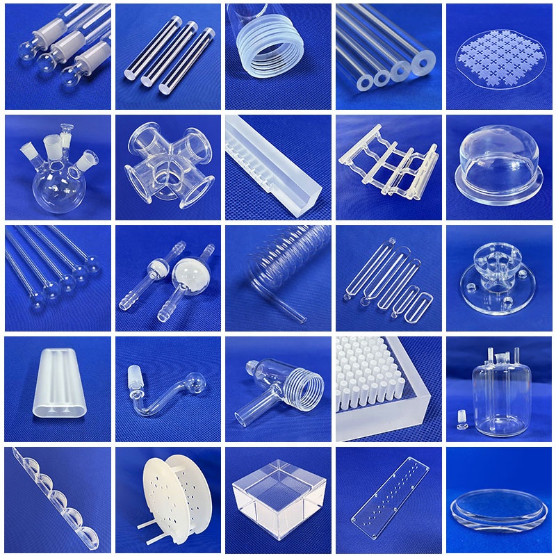
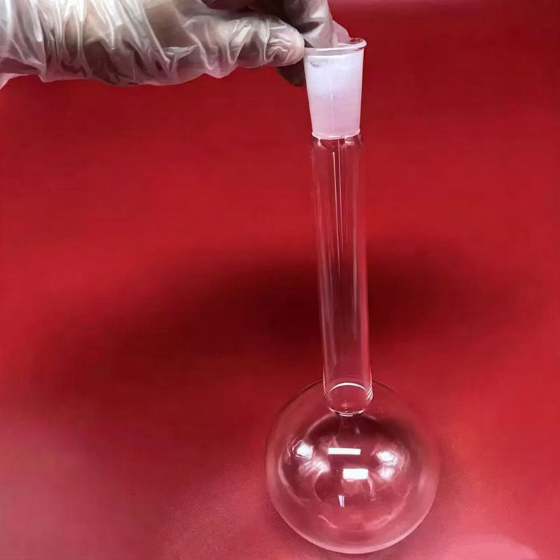
99.99% High-Purity SiO2 High-Temperature Resistant 1200°C Quartz Glass Long-Neck Flask
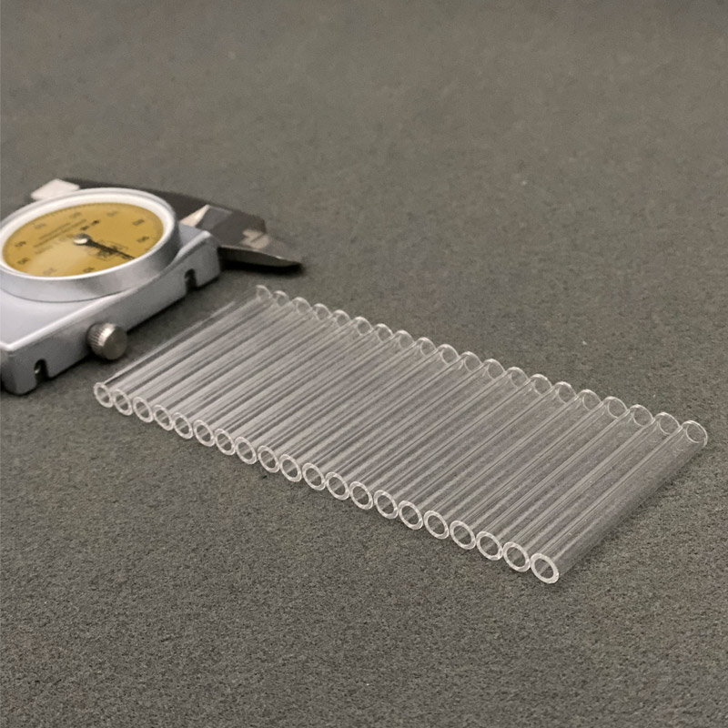
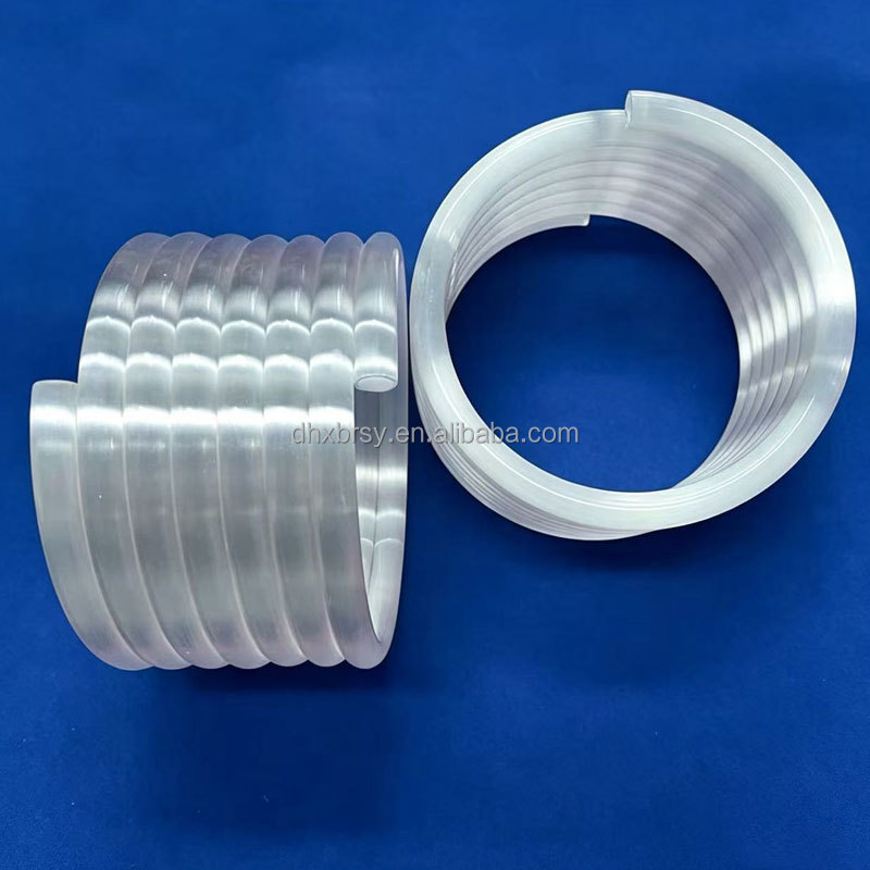
Custom Milky White Opaque Fused Silica Quartz Spiral Tube Helix Coil for Infrared Furnace
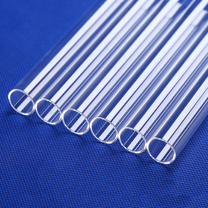
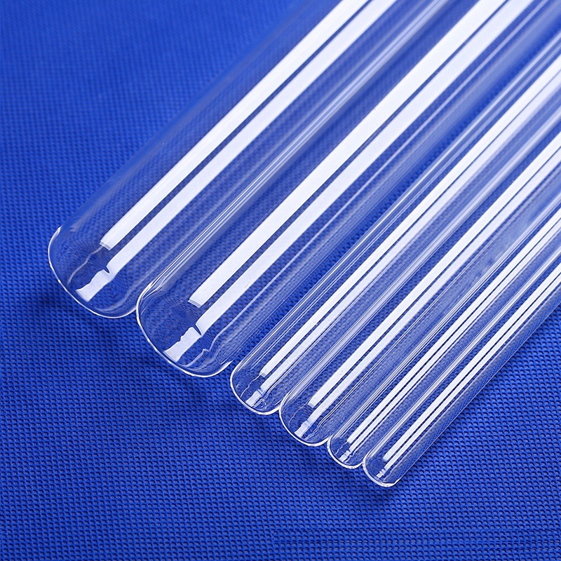
High Precision Clear Quartz Glass Tubing OD 10mm/14mm/20mm Heat Resistant Cleaning Pipeline
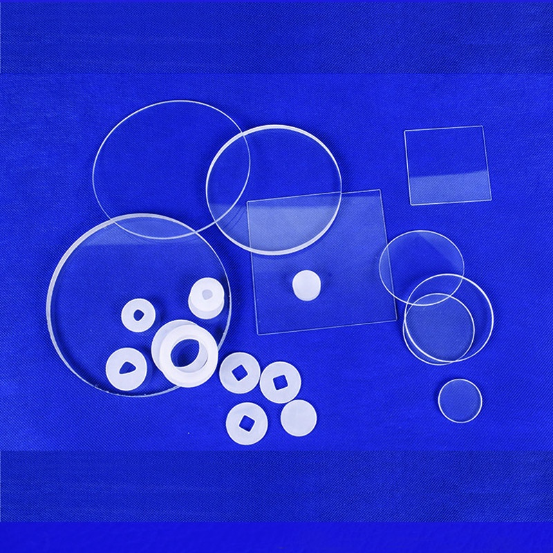
Material Architecture: Synthetic Fused Silica vs. Fused Quartz
In advanced semiconductor, excimer laser, and solar CVD environments, selecting between electrically fused quartz, flame-fused quartz, and synthetic chemical vapor deposition fused silica dictates tool uptime and transmission yield.
| Optical / Thermal Grade | Production Route | Hydroxyl (OH⁻) Level | Transmission Bandwidth | Primary Industrial Vector |
|---|---|---|---|---|
| JGS1 (Synthetic Silica) | SiCl₄ Vapor-Phase Oxidation | < 10 to > 1200 ppm (Controlled) | 185 nm – 2500 nm (Deep UV) | DUV Lithography, Laser Windows, Photomasks |
| JGS2 (Optical Quartz) | High-Purity Quartz Flame Fusion | 150 – 200 ppm | 220 nm – 2500 nm (Near UV / Vis) | UV Curing Tubes, Observation Ports, Jigs |
| JGS3 (Infrared Silica) | Electric Vacuum Melting | < 5 ppm (Water-Free) | 260 nm – 3500 nm (Extended IR) | High-Temp Viewports, IR Pyrometry, Laser Flow Tubes |
| Opaque / Translucent | Controlled Aeration Vitrification | < 30 ppm | Scattered / High IR Emissivity | Furnace Flanges, IR Heating Spirals, Thermal Barriers |
Thermomechanical Immunity
With an extremely low coefficient of thermal expansion (5.5 × 10⁻⁷ /°C from 20°C to 320°C), our components endure rapid immersion from 1100°C into ice water without micro-fracturing or phase transitioning to cristobalite.
Polarization Stress Relief
Every tube and CNC-machined apparatus passes through an automated 1200°C electric annealing cycle followed by cross-polarization photoelastic testing to verify residual internal stress is maintained below 4 nm/cm.
Corrosion & Plasma Inertness
Possessing chemical resistance against all mineral acids (except hydrofluoric and hot phosphoric above 300°C), our semiconductor furnace tubes exhibit negligible dry etching degradation during fluorine and chlorine plasma cleaning.
Vertically Integrated 14,271 m² Facility in Lianyungang
Lovri Quartz operates at the epicenter of China's silica raw material belt. By controlling the entire manufacturing pipeline from raw mineral crushing through 5-axis CNC machining, we eliminate secondary markups and guarantee trace element purity.
End-to-End In-House Manufacturing Verification
Unlike trading entities, Lovri Quartz controls a 12-stage manufacturing chain: raw silica lump selecting → ball-mill pulverizing → secondary high-mesh rescreening → four-stage acid chemical de-ironing → vertical and horizontal tube drawing → automated 1200°C annealing → diamond saw precision slicing → mechanical edge grinding → 5-axis CNC ultrasonic milling → optical flame polishing → deionized ultra-clean batch cleaning → Class 1000 cleanroom packaging.
Third-Party Validation: Our production lines and physical plant have undergone rigorous onsite inspection by SGS Group (Assessment Report: 2025.12.28), confirming our production floor space, advanced CNC machinery, spectrochemical laboratory, and export-compliant pressure testing workflows.
Precision CNC Machining
Multi-axis ultrasonic CNC milling centers facilitate complex hole patterns, wafer boat slots with pitch tolerances under ±0.05 mm, blind tapped threads, and micron-level optical chamfers directly executed on vitreous silica.
Thermal Glassblowing & Lathes
Equipped with large-bore planetary glass lathes, our master technicians fuse custom flanges up to 600 mm OD, multi-bore capillary manifolds, long-neck laboratory flasks, and high-vacuum CVD reaction chambers seamlessly.
Full CE & RoHS Compliance
All quartz products comply with European CE directives (PED 2014/68/EU for pressure apparatus and LVD for quartz heating elements). Materials are RoHS-certified, devoid of restricted lead, cadmium, mercury, or hexavalent chromium compounds.
Future Procurement Trends in High-Purity Fused Silica
As wafer fabrication advances beyond 3nm nodes and high-power industrial fiber lasers surpass 30kW thresholds, the criteria for selecting fused silica components are shifting rapidly.
Transition to Synthetic Plasma Glass
Natural quartz is increasingly reaching its thermal and impurity ceiling in sub-3nm wafer handling. Procurement contracts are aggressively migrating toward synthetic fused silica (JGS1 equivalent) with total metallic impurity levels below 10 ppb to prevent mobile ion migration (Li, Na, K) in high-k dielectrics.
Super-Diameter Diffusion Tubes
With TOPCon and HJT solar cell manufacturers standardizing on 210mm and rectangular silicon wafers, demand has exploded for extra-large diameter quartz furnace tubes (OD > 450 mm). Procurement managers are securing dedicated line capacities to hedge against regional silica supply chain constraints.
Ultra-Low OH Synthetic Windows
For multikilowatt industrial welding and cutting lasers, residual hydroxyl (OH⁻) ions trigger localized bulk thermal absorption, leading to thermal lensing and focal shift. Buyers require documented OH content < 5 ppm coupled with laser damage threshold (LDT) certifications exceeding 20 J/cm².
Low-Carbon Electric Annealing
European and North American OEMs now mandate Scope 1 and Scope 2 emissions audits for fused silica suppliers. Moving away from coal-gas flame heating toward all-electric clean-room furnaces powered by renewable grids has become a prerequisite for Tier-1 supply tenders.
Laser Etched Batch QR Metrology
Standard quality certificates are no longer sufficient. Enterprise procurement now demands micro-laser engraved 2D data-matrix codes on each quartz cylinder or wafer carrier, directly linking the physical item to interferometric homogeneity reports and spectrochemical ICP-MS data.
B2B Procurement Frequently Asked Questions
Practical engineering insights addressing thermal limitations, machining tolerances, stress testing, and international logistics for mission-critical quartz components.
What is the absolute maximum continuous operating temperature for Lovri fused quartz?
Our clear transparent fused quartz products operate continuously up to 1100°C without dimensional deformation. For short durations, peak thermal exposure can safely reach 1300°C. The softening point is 1730°C, and the annealing point is 1215°C. To prevent devitrification above 1150°C, the silica surface must be strictly clean and devoid of alkaline fingerprint oil or dust contamination.
How does your factory verify that quartz parts are free from internal residual stresses?
Following hot working or welding, quartz develops significant localized stress that causes spontaneous catastrophic cracking under heat. Every component in our factory undergoes a multi-hour ramped annealing cycle in dedicated programmable kilns. Each piece is then 100% verified using dual-polarizer photoelastic stress interferometers, ensuring optical retardation is kept below 4–8 nm/cm according to international standards.
What are your standard machining tolerances for CNC quartz wafer carriers and apparatus?
For CNC diamond-milled and slotted components like semiconductor wafer boats and microfluidic flow cells, we maintain linear tolerances of ±0.02 mm and slot pitch tolerances within ±0.03 mm. For raw drawn continuous tubing, outer diameter (OD) and wall thickness tolerances are typically maintained within ±0.1 mm to ±0.2 mm depending on the bore size.
Can you provide material compliance certificates (CE, RoHS, ICP-MS Elemental Analysis)?
Yes. Every production run is supplied with a comprehensive Certificate of Conformance (CoC), raw material purity breakdown via Inductively Coupled Plasma Mass Spectrometry (ICP-MS) demonstrating 99.99% to 99.999% SiO₂ purity, and official RoHS test reports verifying zero hazardous heavy metal contents. CE documentation is provided for quartz assemblies integrating heating or pressure features.
How does your export packaging ensure zero breakage during international air and sea freight?
We use a multi-tier shock-isolation packaging method: parts are sealed in cleanroom PE film, wrapped in heavy-duty impact-dissipating pearl foam (EPE), suspended inside rigid multi-wall inner cartons, and finally packed into heavy fumigated wooden crates lined with high-density polyurethane dampening buffers. Our export transit breakage rate across 40+ countries is <0.1%.
What is the typical prototyping lead time and minimum order quantity (MOQ)?
Because we are a direct manufacturer with stocked raw ingots and drawn tubing, our MOQ for standard plates, rods, and tubes is 1 piece. Rapid prototyping of custom components according to customer drawings (CAD / STEP / DWG / PDF) typically ships within 7 to 10 working days. Scaled volume production batches are completed within 2 to 3 weeks.
Connect with Our Senior Quartz Applications Engineering Team
Whether you need urgent semiconductor wafer boats, custom JGS1 optical sight windows, or large-bore furnace tubes manufactured to rigid tolerances, submit your technical drawings for an immediate manufacturability review and factory-direct pricing quote.
Get a Quote