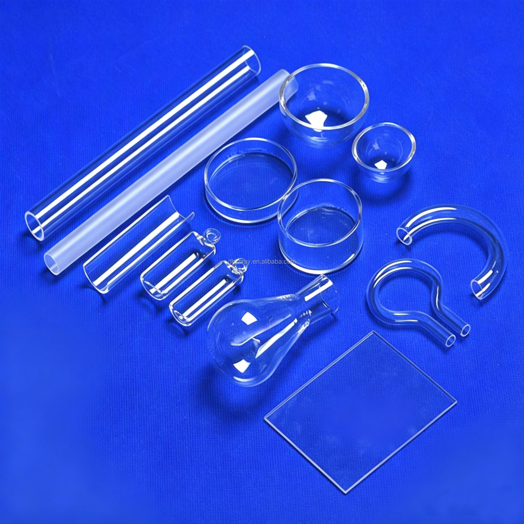
Featured Fused Silica & Quartz Components
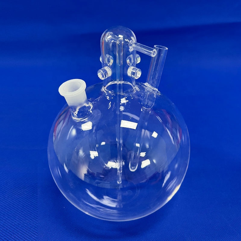
Direct factory production lines for semiconductor wet benches, high-energy laser cavities, chemical vapor deposition (CVD), and deep ultraviolet (DUV) transmission windows.
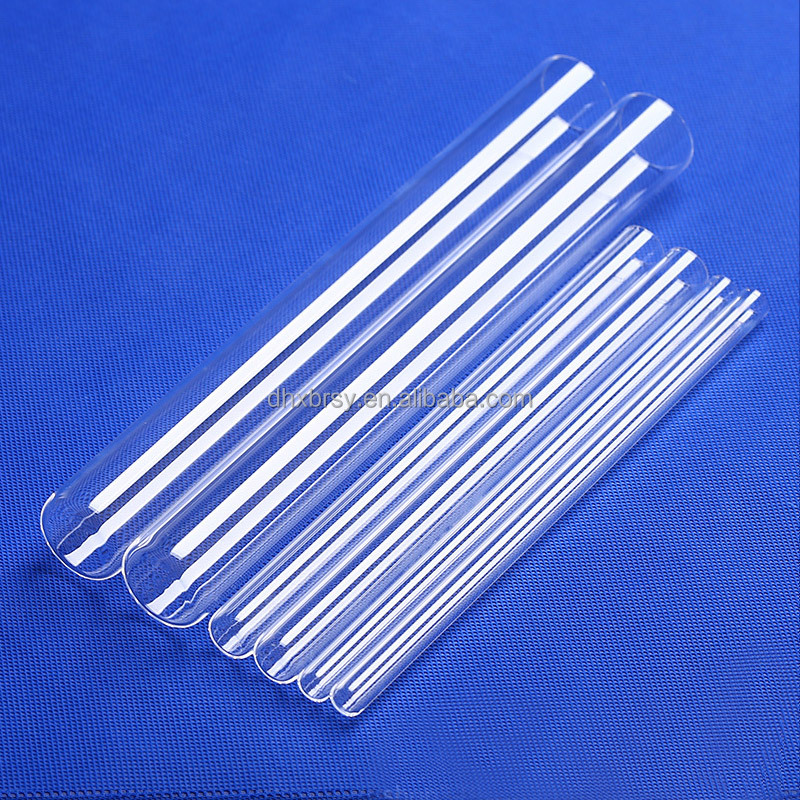
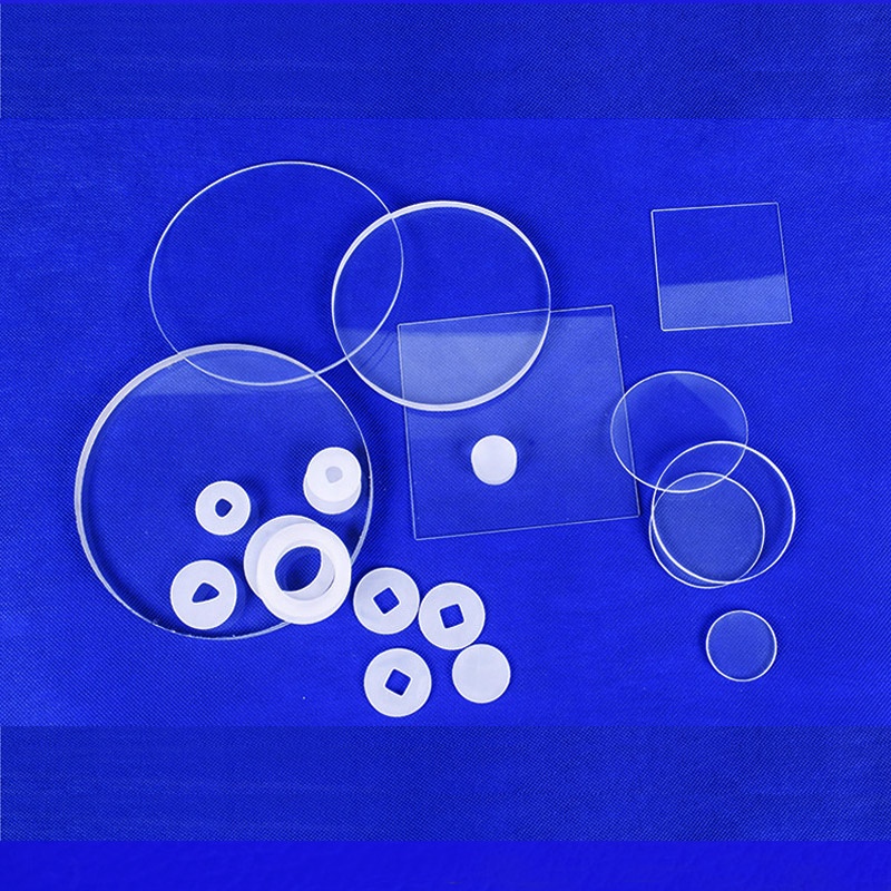
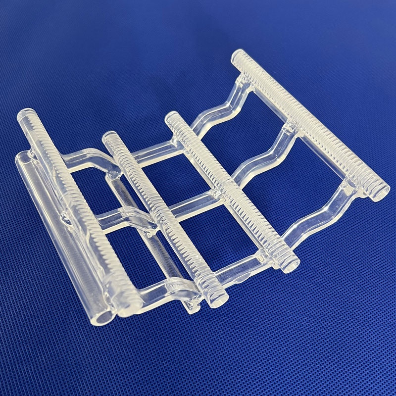
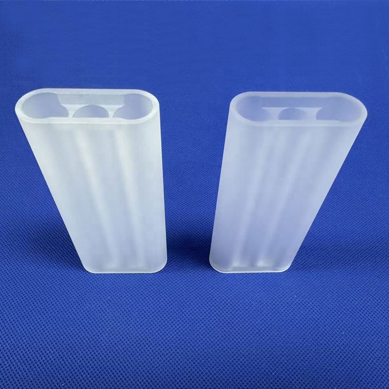
Material Science of Fused Silica Sheets: Structural Uniformity and Defect Control
In critical semiconductor lithography, high-power fiber laser optics, and industrial reactor windows, optical components are subjected to punishing mechanical stresses, high thermal gradients, and intense photon flux. Standard borosilicate, aluminosilicate, or commercial soda-lime glass structures catastrophically fail under rapid cycling due to their high thermal expansion coefficients and intrinsic alkali metal impurities. Fused silica—amorphous silicon dioxide (SiO₂ ≥ 99.99%)—represents the engineering zenith for transmissive optics and thermal barrier substrates.
As a premier CE Certified Fused Silica Sheet Manufacturer and Exporter, Lovri Quartz controls the synthetic and thermal synthesis route to eliminate macroscopic inclusions, striae, and structural birefringence. The performance disparity between natural fused quartz (manufactured via electric or flame melting of natural quartz sands) and synthetic fused silica (synthesized from the chemical vapor deposition or gas-phase oxidation of silicon halides like SiCl₄) dictates optical transmission bands, laser damage thresholds, and hydroxide (OH⁻) absorption signatures.
JGS1: Synthetic UV Fused Silica
Formed by chemical vapor deposition using ultra-pure synthetic raw precursors. Exhibits zero fluorescence in the ultraviolet spectrum, virtually free from bubble classes, with high transmissive efficiency extending from 185 nm to 2500 nm. Engineered specifically for excimer laser output optics, UV lithography masks, and high-energy spectrophotometer viewports.
JGS2: Optical Grade Quartz Glass
Produced via continuous hydrogen-oxygen flame fusion using selected high-grade crystal sands. Provides stable broadband transmission from 220 nm to 2500 nm with excellent macroscopic homogeneity and high mechanical toughness. Ideal for sight glasses, industrial plasma viewing windows, ultraviolet sterilizing sleeves, and chemical process reactors.
JGS3: Infrared Electrically Fused Silica
Synthesized in a vacuum electric resistance melting environment, keeping the hydroxyl (OH⁻) content strictly below 5 ppm. This process eliminates the broad water-absorption bands typically seen around 2.73 μm, enabling high transmissive fidelity across the near-to-mid infrared band from 260 nm up to 3500 nm. Crucial for thermal IR imaging, furnace sight-ports, and pyrometry.
Standardized Physical, Optical & Thermal Properties Matrix
| Physical Property Characteristic | Measurement Standard | Fused Quartz (JGS2/Electrically Fused) | Synthetic Fused Silica (JGS1) |
|---|---|---|---|
| Chemical Composition & Purity | ICP-OES / GD-MS Spectrometry | SiO₂ ≥ 99.99% | SiO₂ ≥ 99.9999% (Ultra-Trace Impurities) |
| Hydroxyl (OH⁻) Ion Content | FTIR Absorption Spectrum | 150 – 300 ppm (Flame) / < 5 ppm (Electric) | < 1200 ppm (High OH) / < 10 ppm (Low OH) |
| Density (ρ) | Archimedes Immersion Method | 2.201 g/cm³ | 2.203 g/cm³ |
| Coefficient of Thermal Expansion (CTE) | Dilatometry (20°C to 320°C) | 5.5 × 10⁻⁷ K⁻¹ | 5.2 – 5.4 × 10⁻⁷ K⁻¹ |
| Annealing Point / Softening Point | Beam Bending Viscometry | 1140°C / 1730°C | 1180°C / 1730°C |
| Refractive Index ($n_d$ at 589.3 nm) | V-Block Pulfrich Refractometry | 1.4585 | 1.4584 |
| Optical Homogeneity (Δn) | Laser Phase-Shifting Interferometry | Class D / C (≤ 1 × 10⁻⁴) | Class A / B (≤ 2 × 10⁻⁶) |
| Surface Flatness & Surface Quality | Zygo GPI Interferometer / MIL-PRF-13830B | λ/4 to λ/2, Scratch-Dig 60/40 | Up to λ/10, Scratch-Dig 20/10 or 10/5 |
Why Global Tier-1 Buyers Partner with Lovri Quartz
Combining Lianyungang’s raw geological quartz cluster with precision CNC cold-machining and certified cleanroom annealing protocols.
Headquartered in the Tuofeng Industrial Park, Lianyungang (Jiangsu Province)—the epicenter of the world's most concentrated quartz processing supply network—Lovri Quartz Products Co., Ltd. controls the complete vertical processing chain. Unlike trading intermediaries who purchase standard un-annealed quartz blanks from third-party melting yards, our facility operates an SGS-audited, 14,271 m² production base.
By maintaining complete in-house capabilities from raw silica crushing, acid pickling (HF/HCl chemical purification), and horizontal tube/ingot drawing to secondary CNC profile milling, flame fire-polishing, and ultrasonic optical packaging, we provide predictable batch-to-batch repeatability. Residual stress within fused quartz is the primary culprit behind spontaneous optical distortion and vacuum fracture; every single lot fabricated in our workshops undergoes polariscopic stress relief verification to ensure that optical path difference (OPD) remains below 5 nm/cm.
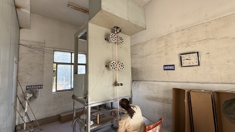
SGS Verified 14,271 m² Facility
Onsite assessed facility with clean-assembly zones and automated multi-axis grinding benches.
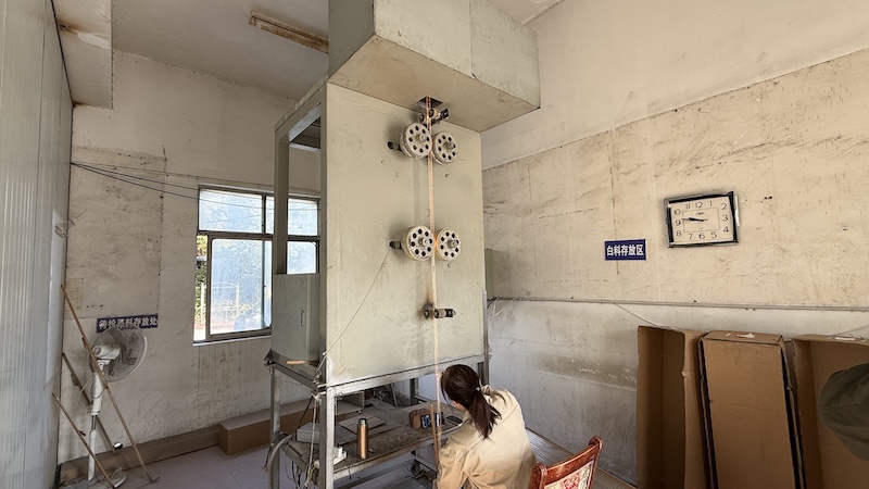
Continuous Ingot & Tube Drawing
Electric vacuum heating and flame sizing guaranteeing continuous wall thickness and outer diameter integrity.
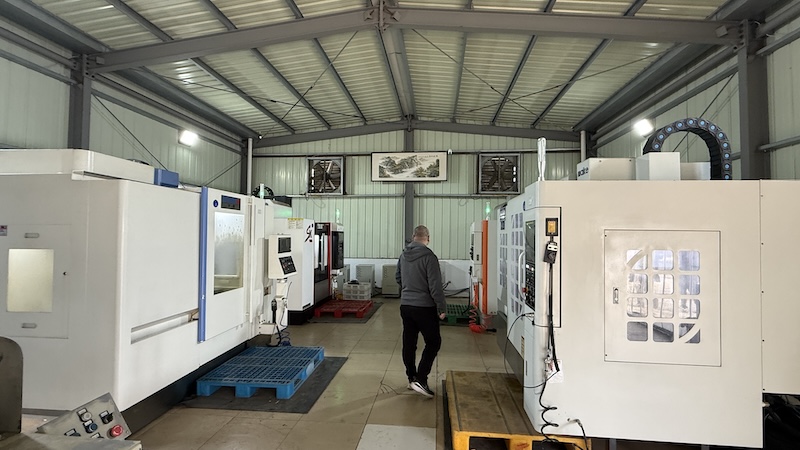
5-Axis CNC Precision Machining
Diamond-tooled edging, beveling, micro-hole laser drilling, step milling, and ultra-flat surface grinding.
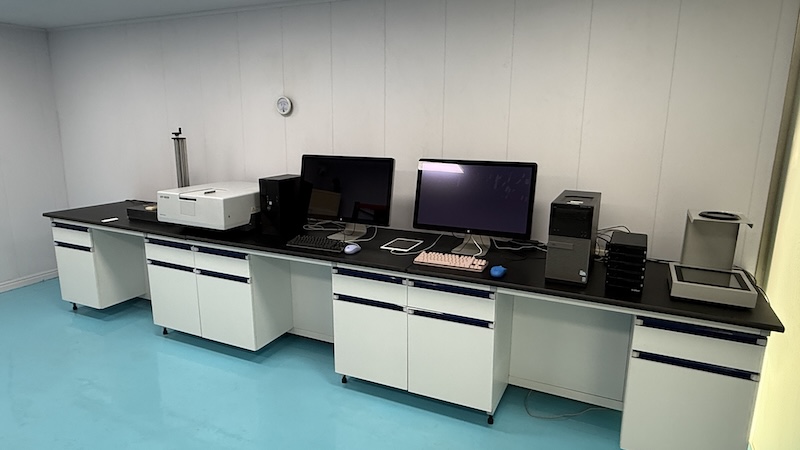
Optical Metrology & Quality QA
Spectrophotometer transmittance validation, polarization stress testing, and surface roughness interferometry.
Fused Silica Sheet Procurement Trends (2025–2030)
Navigating evolving technological shifts, purity mandates, and supply-chain risk mitigation in advanced manufacturing sectors.
Sub-Nanometer Optical Finish
With high-power industrial fiber lasers surpassing 30 kW and EUV beam lines deploying complex collectors, buyers are shifting toward Chemical Mechanical Planarization (CMP) with surface roughness Ra < 0.2 nm to suppress laser-induced damage thresholds (LIDT).
Ultra-Thin Substrates (≤0.2mm)
Accelerating demand from microfluidics, MEMS encapsulation, and direct wafer-level packaging requires ultra-thin sliced fused silica sheets from 0.1 mm to 0.5 mm with tight thickness variation (TTV < 2 μm) and minimal edge chipping.
Near-Net CNC Integration
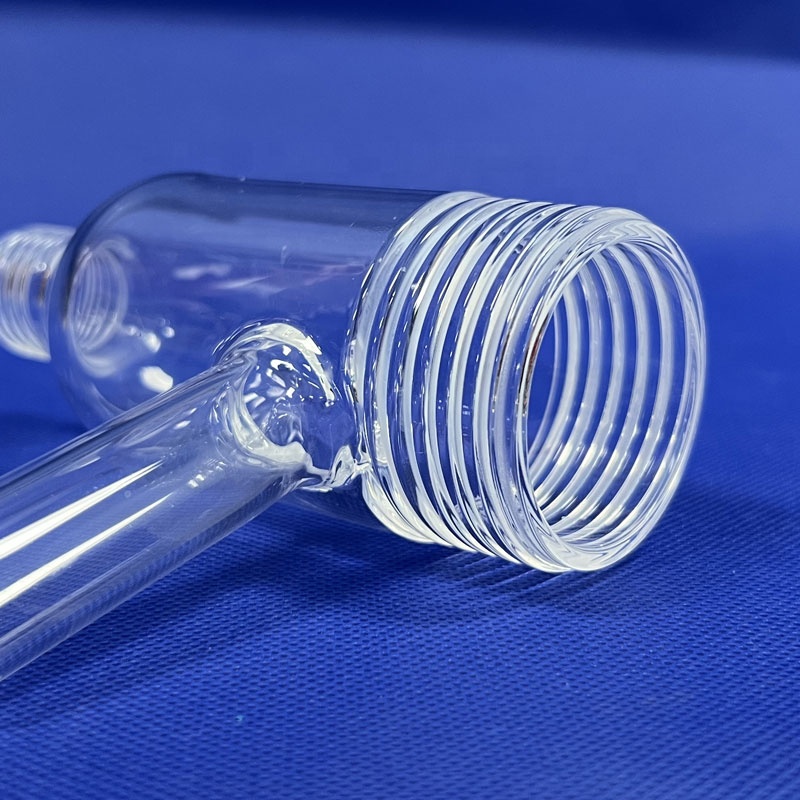
Procurement teams are cutting assembly costs by ordering monolithic fused quartz structures. Instead of gluing or clamping multiple glass parts, multi-axis CNC machines mill threaded ports, stepped shoulders, and sealing O-ring recesses directly onto the sheets.
ESG & Traceability Auditing
Stringent EU cross-border carbon mandates and RoHS 2.0/REACH certifications require transparent mineral origin reporting and closed-loop acid recycling during the purification process. Audited suppliers like Lovri Quartz offer complete material chain of custody.
Technological Trajectory: Where Fused Silica Is Replacing Classical Ceramics & Sapphire
The global technical ceramics and glass market is experiencing a profound architectural shift. While sapphire (monocrystalline Al₂O₃) has long been favored for scratch resistance and high-temperature integrity, its prohibitive cost, optical anisotropy (birefringence), and high thermal expansion coefficient make it prone to thermal cleavage when subjected to localized heating. Fused silica sheets provide an isotropic alternative with virtually zero thermal shock risk, exceptional dielectric breakdown voltage (> 25 kV/mm), and broad spectral transparency.
In the semiconductor fabrication space, transition to 300 mm wafer processing and atomic layer deposition (ALD/CVD) creates corrosive plasma environments where traditional borosilicate observation ports degrade in hours. Fused silica sheets with 99.99% purity resist atomic chlorine, fluorine plasma, and strong mineral acids (except hydrofluoric acid), making them the industry standard for observation viewports, wafer boats, and plasma chamber liners.
Similarly, in biomedical and analytical fields, high-throughput gene sequencing and laser-induced fluorescence spectrometry require quartz microplates, capillary flow cells, and observation plates with near-zero background autofluorescence. Synthetic fused silica sheets eliminate the heavy-metal luminescence common in cheaper glass grades, ensuring optimal signal-to-noise ratios in detection apparatus.
Frequently Asked Technical & Procurement Questions
Authoritative guidance on dimensional limits, surface specifications, thermal limits, and logistics protocols.
Q1: How does CE marking apply to industrial fused silica plates and components?
CE certification confirms that our fused silica products comply with the essential health, safety, and environmental protection requirements of relevant European Directives, specifically regarding low-voltage pressure chamber apparatus, high-temperature equipment enclosure standards, and hazardous material restrictions (RoHS 2011/65/EU and REACH (EC) No 1907/2006). Comprehensive Certificates of Conformity (CoC) and material safety datasheets (MSDS) are provided with every export shipment.
Q2: What are the realistic machining tolerances achievable for custom cut-to-size quartz sheets?
Using diamond multi-wire slicing, CNC ultrasonic drilling, and high-speed CNC machining centers, Lovri Quartz typically achieves ±0.05 mm on length and width dimensions. For precision optical windows and wafer carrier substrates, grinding and double-side lapping yield thickness tolerances of ±0.01 mm, surface parallelism ≤ 10 arcseconds, and edge chamfers of 0.2–0.5 mm × 45° to eliminate micro-chipping and stress concentration points.
Q3: Can transparent fused quartz sheets withstand sudden thermal shock from 1100°C to water quenching?
Yes. Fused quartz exhibits an extraordinarily low linear thermal expansion coefficient of approximately 5.5 × 10⁻⁷ /°C. A standard test piece heated to 1100°C in an industrial muffle furnace can be immediately immersed into 20°C ambient water without structural fracture or micro-crack propagation. However, operating quartz continuously above 1150°C in the presence of surface alkali contaminants can induce devitrification (nucleation of cristobalite), which reduces thermal shock resistance.
Q4: What surface quality standards do you inspect by default for laser and optical applications?
Our default commercial optical polishing complies with MIL-PRF-13830B Scratch-Dig 60/40 or ISO 10110 standards. For high-energy laser optics, UV beam splitters, and critical lithography windows, we provide precision pitch polishing achieving Scratch-Dig 20/10 or 10/5, with surface roughness Ra < 0.5 nm (measured via white-light optical profilometer) and transmitted wavefront distortion ≤ λ/4 at 632.8 nm.
Q5: What is the protocol for preventing transit breakage during international air and sea freight?
Quartz glass is classified as fragile high-value cargo. Lovri Quartz employs a 4-tier packaging protocol: (1) dust-free protective static film wrapping or optical lens tissue; (2) vacuum-sealed moisture-barrier bagging; (3) high-density form-fitting polyethylene (EPE) shock-absorbing foam nests; and (4) reinforced fumigated solid-plywood crates with impact/tilt indicators. Our breakage rate across over 40 export destinations is under 0.08%.
Q6: What is the difference between fire-polished, mechanically polished, and ground quartz edges?
Ground edges (matte finish) provide precise dimensional control and cost efficiency for internal furnace liners. Mechanical optical polishing ensures mirror transparency and flatness for viewing ports and clamping edges. Fire-polishing involves running a hydrogen-oxygen torch across the diamond-cut edge to melt away microscopic fissures, increasing mechanical tensile edge strength by over 40% to prevent stress fractures in pressurized vacuum environments.
Q7: Can you fabricate integrated fused silica components directly from STEP or DWG engineering CAD files?
Yes. Our in-house engineering and tooling center works natively with 3D CAD formats (STEP, IGES) and 2D vector files (DWG, DXF, PDF). Our CAM software translates CAD geometries directly into multi-axis CNC toolpaths for drilling circular or irregular blind holes, machining internal O-ring seal grooves, counter-boring screw recesses, and milling complex curved profiles.
Q8: What is the typical Minimum Order Quantity (MOQ) and production turnaround for custom prototypes?
To support corporate R&D centers, universities, and prototype validation, our factory maintains a low MOQ policy (as low as 1 to 5 pieces for custom CNC machined parts and sheet prototypes). Standard rapid tooling prototypes ship within 7–10 working days, while volume production runs (hundreds to thousands of sheets) are completed within 3–4 weeks depending on raw ingot processing requirements.
Submit Your Engineering Drawings for Immediate Quotation
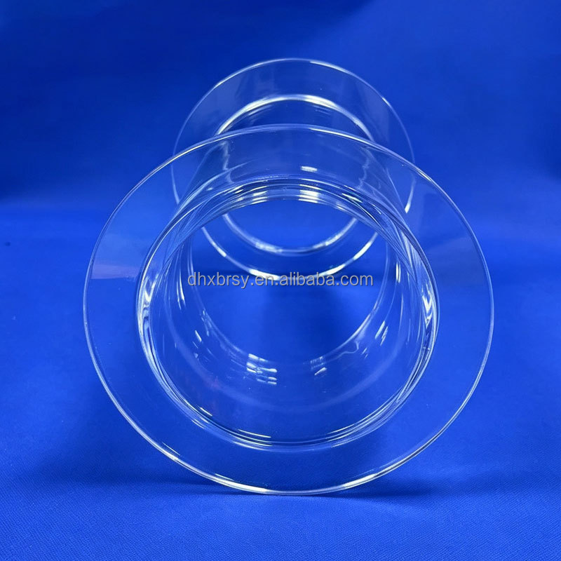
Whether you require standard 100mm × 100mm JGS1 UV optical windows, 0.2mm ultra-thin semiconductor substrates, or custom double-flanged CVD vacuum chambers, our application engineers provide a detailed technical review, tolerance optimization, and commercial quotation within 24 hours.