
≥99.99%
SiO₂ Chemical Purity
14,271 m²
SGS Audited Facility
λ/10
Surface Wavefront Accuracy
1100 °C
Continuous Operating Temp
Precision Engineering Matrix
High-Performance Quartz Optical Plates & Core Assemblies
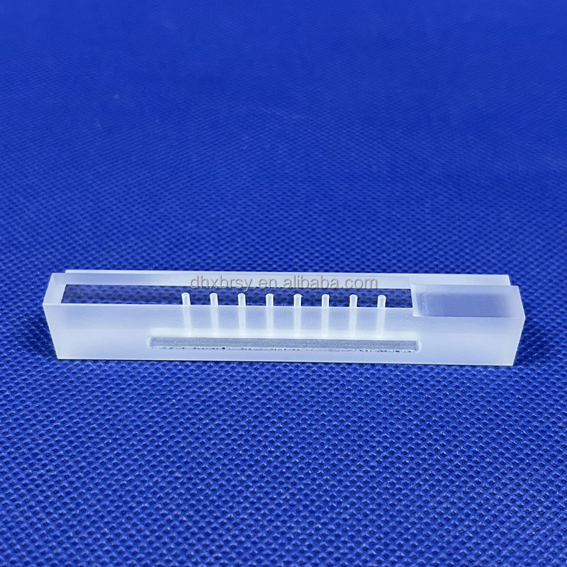
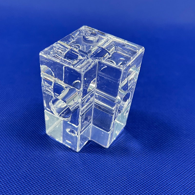
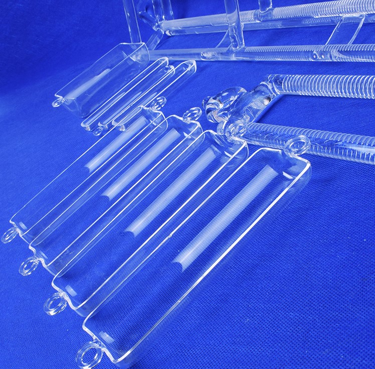
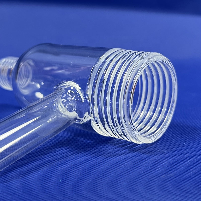
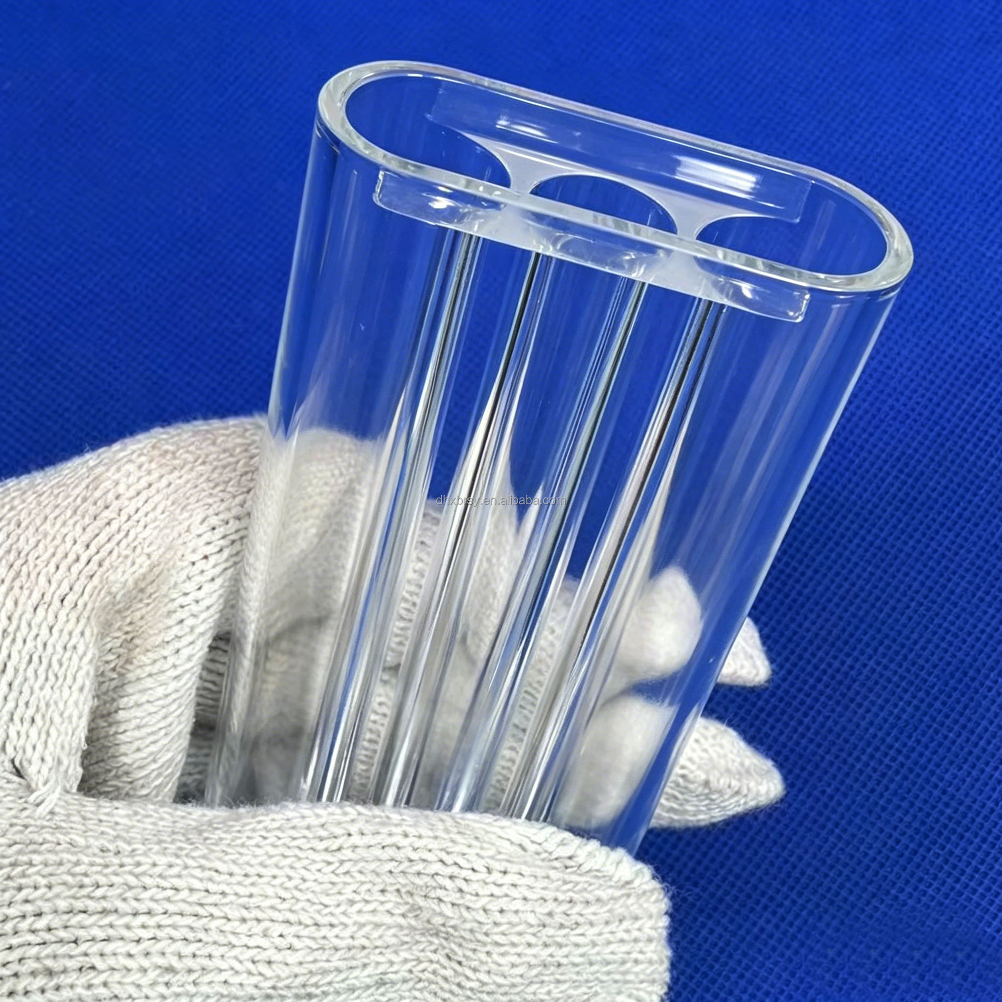
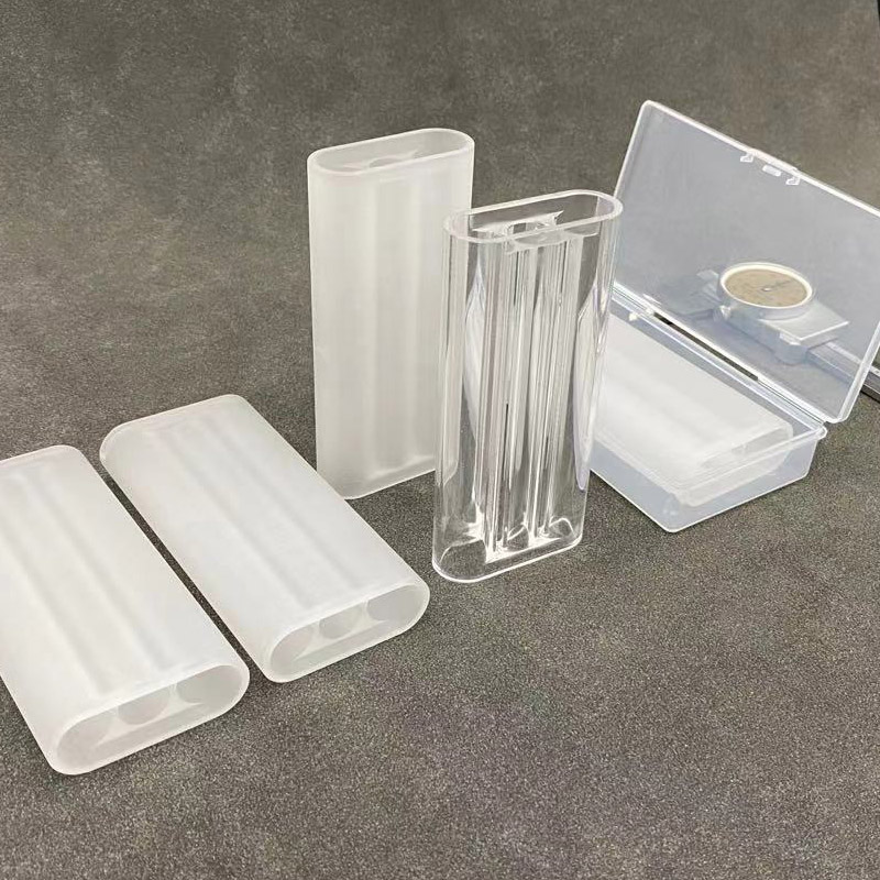
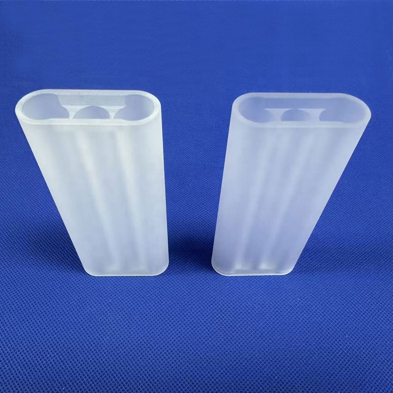
Engineered for high-power laser optics, semiconductor wafer carriers, analytical spectroscopy, and extreme thermal fluidic reactors. Sourced from high-purity crystalline quartz sand with zero subsurface micro-fracturing.
Material Science Engineering
Optical Grade Differentiation: JGS1 vs. JGS2 vs. JGS3
In high-precision optical plate manufacturing, selecting the appropriate synthetic or natural silica matrix dictates spectral performance, laser-induced damage thresholds (LIDT), and chemical stability across operating wavelengths.
JGS1: Synthetic Fused Silica (Far UV)
Manufactured through chemical vapor deposition of SiCl4, JGS1 exhibits exceptional optical transmission from 185 nm to 2500 nm. Completely bubble-free with virtually zero metallic impurities, it provides negligible fluorescence under ultraviolet excitation, making it the primary standard for excimer laser optical windows, photolithography mask blanks, and UV spectrophotometer flow plates.
JGS2: Flame-Fused Optical Quartz (UV-Vis)
Synthesized by melting selected natural crystal quartz via oxyhydrogen flame fusion, JGS2 provides balanced optical characteristics within the 220 nm to 2500 nm range. While retaining robust thermal stability and high mechanical strength, its cost-effective profile renders it suitable for high-intensity discharge sight glasses, furnace viewports, plasma etching windows, and standard optical filters.
JGS3: Electrically Fused Silica (Infrared)
Produced via vacuum electrical resistance smelting, JGS3 eliminates hydroxyl (-OH) radicals, yielding water band absorption suppression around 2.73 μm. It delivers transmission extended into the mid-infrared spectrum up to 3500 nm. It is applied in infrared pyrometry, gas detection absorption cells, thermal imaging subassemblies, and high-temperature optical sensor enclosures.
| Physical / Optical Parameter | JGS1 (Far UV Grade) | JGS2 (Standard Optical) | JGS3 (Infrared Grade) | Test Standard / Metrology |
|---|---|---|---|---|
| Spectral Window (T ≥ 85%) | 185 nm – 2500 nm | 220 nm – 2500 nm | 260 nm – 3500 nm | PerkinElmer Lambda 1050+ |
| Hydroxyl (-OH) Content | ≤ 1200 ppm (Hydrated) | 150 – 200 ppm | ≤ 5 ppm (Water-Free) | FTIR Infrared Spectroscopy |
| Refractive Index (nd, 589.3 nm) | 1.4585 | 1.4585 | 1.4584 | Precision V-Block Refractometer |
| Coefficient of Thermal Expansion | 5.5 × 10⁻⁷ / °C (20–320°C) | 5.5 × 10⁻⁷ / °C | 5.4 × 10⁻⁷ / °C | Dilatometric Metrology |
| Laser Induced Damage Threshold (LIDT) | > 15 J/cm² @ 1064nm, 10ns | > 7.5 J/cm² @ 1064nm, 10ns | > 5.0 J/cm² @ 1064nm, 10ns | ISO 21254 Single/Multi-shot |
| Surface Quality (Scratch-Dig) | 10-5 to 20-10 | 40-20 to 60-40 | 60-40 | MIL-PRF-13830B Micro-inspection |
Procurement Intelligence 2026-2030
Strategic Trends Shaping Quartz Optical Component Sourcing
Semiconductor nodes transitioning below 3nm, coupled with kW-class industrial fiber laser optics and orbital space communication setups, demand unprecedented evolution in Chinese fused silica supply networks.
Trend 01 • Semiconductor
Large-Format Ultra-Flat Substrates
Next-generation photolithography and wafer-level packaging necessitate fused quartz carrier plates with total thickness variation (TTV) under 1.5 μm across Ø300mm to 450mm formats, demanding double-sided chemical mechanical planarization (CMP).
Trend 02 • Industrial Laser
Sub-ppm Absorption & Thermal Lensing
As multi-kilowatt CW fiber lasers become standard in automotive manufacturing and welding, optical windows must eliminate bulk absorption below 0.5 ppm/cm to prevent focal shift, thermal stress cracking, and beam divergence distortion.
Trend 03 • Metrology
Integrated Stress Birefringence Mapping
Global optical system assemblers no longer accept simple polariscope certification. Procurement specifications now mandate automated polarimetric birefringence mapping (≤ 2 nm/cm residual path difference) per optical component.
Trend 04 • Life Sciences
Monolithic Microfluidic Fabrication
The convergence of lab-on-a-chip and bio-optics drives demand for precision laser-etched, ultrasonically milled, and fusion-bonded multi-layer fused quartz micro-reactors free from autofluorescence under laser-induced fluorescence (LIF) detection.
Lianyungang Cluster Manufacturing
Vertical Processing Integrity: From Raw Silica to Polished Plate
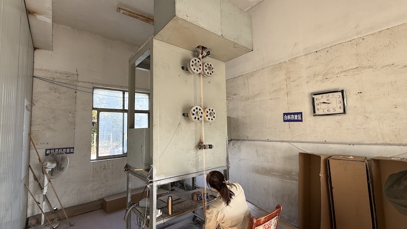
Operating in Lianyungang, China—the hub of high-purity quartz reserves and thermal processing infrastructure—Lovri Quartz Products Co., Ltd. controls the complete manufacturing cycle. By managing everything from natural quartz lump sizing, crushing, and high-temperature chemical acid pickling to computer-controlled thermal annealing and 5-axis CNC diamond grinding, we eliminate third-party raw stock contamination.
Our SGS-audited 14,271 m² production facility houses modern gas-fired hot-pressing kilns, continuous drawing towers, and cleanroom optical polishing lines. This vertical integration allows us to achieve 99.99% SiO₂ purity consistently, maintain tight dimensional tolerances, and provide full spectral transmission and chemical traceability on every export batch.
01
Silica Acid Leaching
Multi-stage HF & HCl acid leaching removes metallic trace elements (Fe, Cu, Ti, Cr) below 15 ppm total impurity.
02
Vacuum Annealing
1200 °C programmed ramp-down thermal annealing cycles relieve structural strain and prevent fracture propagation.
03
Multi-Axis CNC Grinding
Diamond-tooled ultrasonic CNC machining executes edge beveling, blind hole milling, slotting, and contour profiling.
04
Precision CMP Polishing
Cerium oxide & colloidal silica double-sided polishing provides surface roughness (Ra) down to < 0.5 nm.
05
Polarimetric Strain Testing
100% batch validation under cross-polarized light detects residual stress patterns and optical homogeneity limits.
06
Cleanroom Vacuum Packaging
Ultrasonic solvent cleaning, DI water rinsing, and anti-static vacuum wrapping in Class 1,000 cleanrooms.
Direct Supplier Insights
Frequently Asked Technical & Procurement Questions
Clear, engineering-focused answers to guide cross-border procurement teams through material qualification, fabrication tolerances, and logistics compliance.
Q: What is the practical thermal limit difference between fused quartz and borosilicate?
Fused quartz offers a continuous operating threshold of 1100 °C and short-term limit of 1300 °C, with a softening point of approximately 1730 °C. Borosilicate glass fails above 450–500 °C. Furthermore, quartz exhibits an ultra-low thermal expansion coefficient of 5.5 × 10⁻⁷ / °C—roughly one-sixth that of borosilicate—allowing it to withstand immediate water immersion quenching from 1000 °C without thermal shock fracturing.
Q: How do I determine whether my application needs JGS1 or JGS2?
The decision hinges on operating wavelength and laser fluence. For deep UV transmission between 185 nm and 250 nm, excimer laser applications (193 nm, 248 nm), or zero-autofluorescence spectroscopy, JGS1 is strictly required. For visible to near-infrared optics, UV curing lamps (365 nm), industrial sight windows, and general chemical viewports, JGS2 provides equivalent structural and thermal performance at approximately 30–40% lower material expense.
Q: What surface flatness and scratch-dig tolerances can your CNC optical line achieve?
Our precision optical polishing workshops achieve optical surface flatness down to λ/10 (λ = 632.8 nm) per 100mm diameter aperture, with parallelism better than 5 arcseconds and thickness tolerance within ±0.01 mm. Scratch-dig ratings adhere strictly to MIL-PRF-13830B or ISO 10110 standards, achieving 20-10 or 10-5 for critical high-power laser and photolithography optics.
Q: How do you prevent internal mechanical stress from causing in-service cracking?
All raw blanks, drawn tubes, and CNC-cut quartz plates undergo secondary programmable annealing in computerized electrical resistance furnaces at 1215 °C, followed by a controlled ramped cool-down cycle. Each finished lot is inspected under transmission polariscopes to verify that residual optical path difference caused by internal strain remains below 2 to 5 nm/cm.
Q: Can you process custom features such as step holes, threads, and micro-channels?
Yes. We specialize in custom CNC quartz component machining based on client STEP, DWG, DXF, or PDF engineering drawings. Our facility operates multi-axis high-speed machining centers equipped with diamond drills, diamond grinding pins, and ultrasonic vibration tools, enabling precision counterbores, inner/outer threads, slotted carrier combs, and laser-polished microfluidic paths.
Q: What packaging protocols are used to guarantee zero transit breakage for international orders?
Optical components are cleaned in ultrasonic deionized water baths, enclosed in anti-static dust-free PET membranes, and surrounded by custom high-density CNC cut EVA foam slots. The assemblies are then housed in multi-layer corrugated boxes and reinforced within export-grade plywood crates, ensuring impact absorption during international air, sea, and courier transport.
Initiate Your Optical Quartz Engineering Inquiry
Consult with our quartz engineering specialists for custom optical plate prototyping, JGS1/JGS2/JGS3 raw material selection, or volume OEM supply contracts. Get technical feedback within 24 hours.