99.99% SiO₂
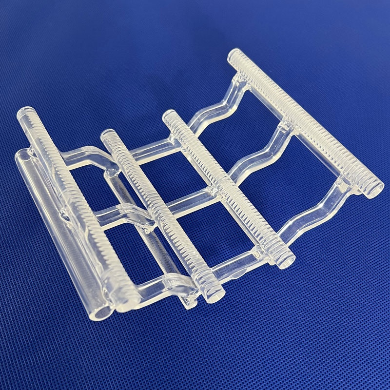
Certified 99.99% SiO₂ high-purity thermal and optical components manufactured under strict cleanroom conditions for critical wafer processing, deep UV lithography, and high-intensity industrial heating.
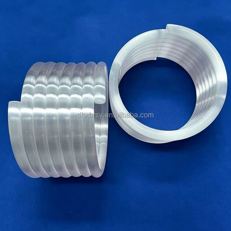
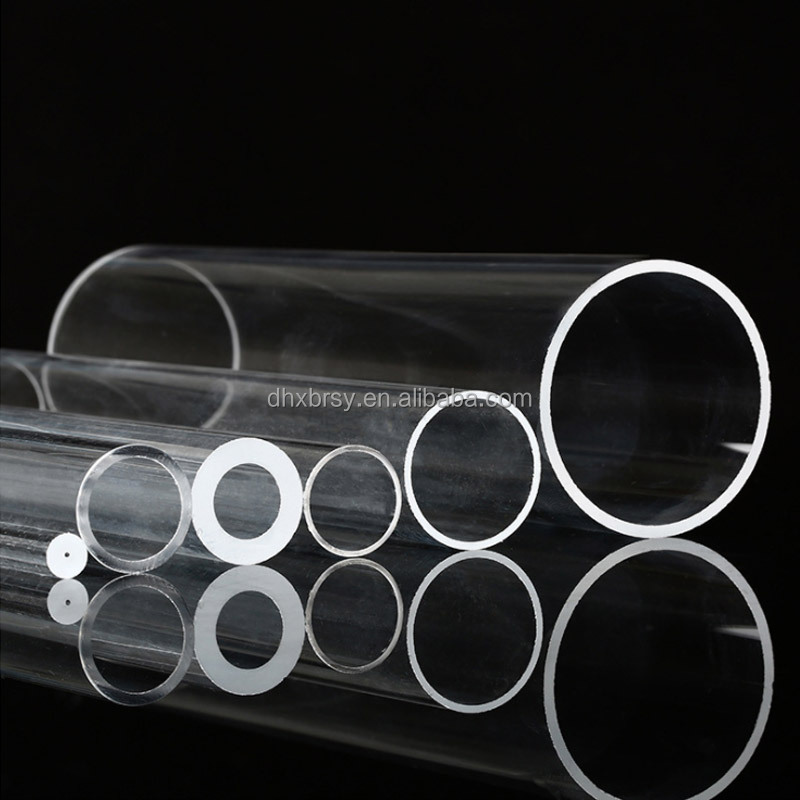
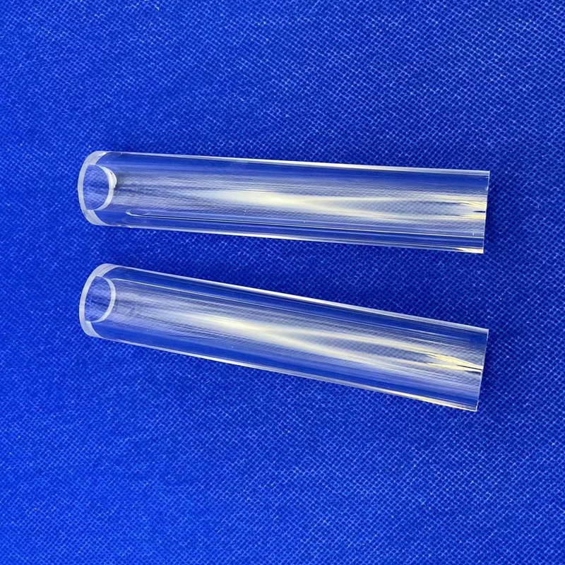
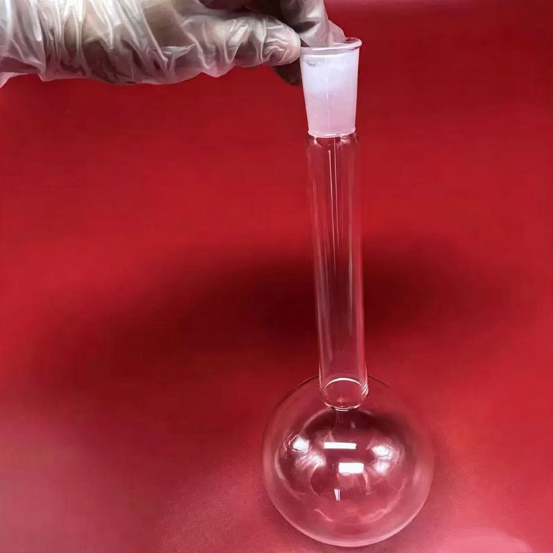
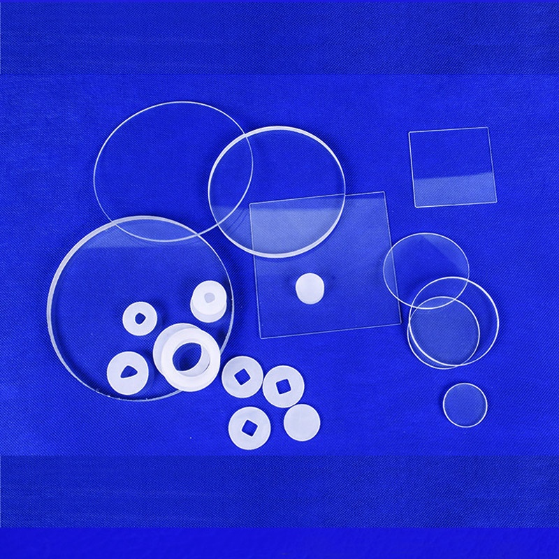
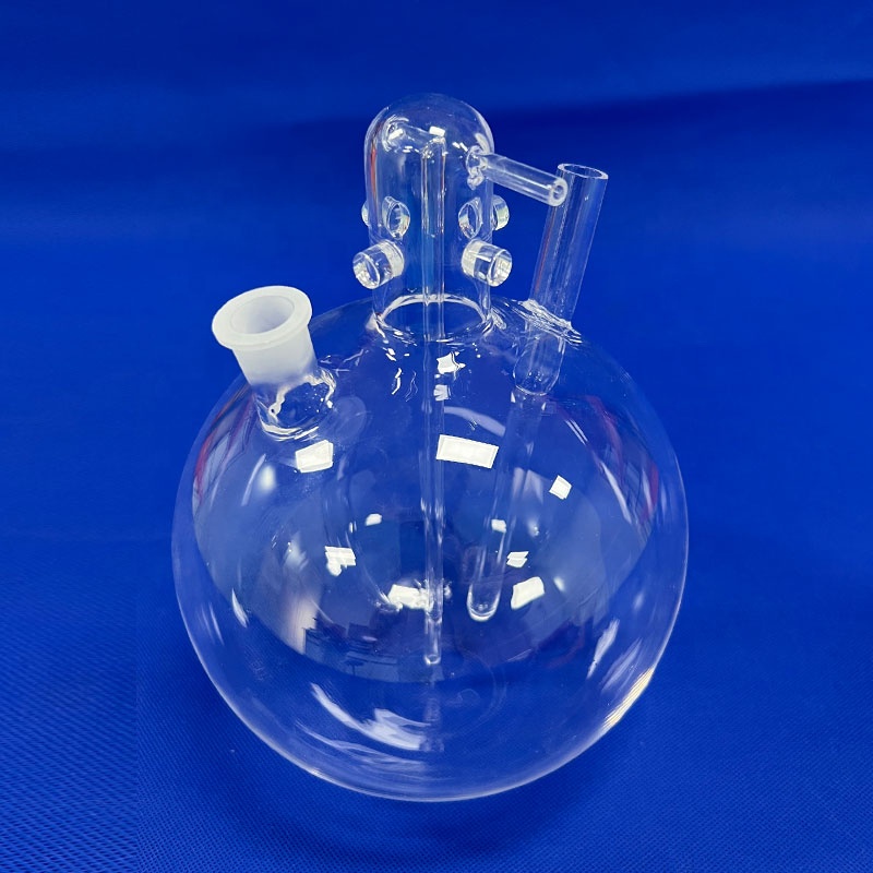
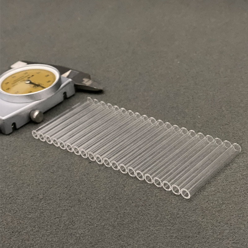
Operating from Lianyungang, China's premier high-purity silica cluster, Lovri Quartz controls the end-to-end processing pipeline—from raw mineral refinement to CNC micron-level micro-fabrication.
In-house calcination, acid pickling, and fine screening eliminate iron, alkali, and metallic inclusions directly at the crystal lattice level.
Diamond ultrasonic drilling, precision perimeter step beveling, surface micro-slotting, and double-sided planetary optical polishing.
100% polarization polarimeter verification after vacuum annealing eliminates brittle failure risks under extreme thermal cycling.
Custom-cut dual-density non-shedding foam liners within fumigated marine plywood cases guarantee zero micro-fractures in international transit.
Selecting the precise optical material grade is essential to prevent bubble-induced laser scattering, UV solarization degradation, or early devitrification during furnace runs.
| Optical Grade | Manufacturing Method | Transmittance Band | OH Content (PPM) | Primary Industrial Application |
|---|---|---|---|---|
| JGS1 (Synthetic) | Chemical Vapor Deposition (SiCl₄) | 185 nm – 2500 nm (Deep UV) | < 5 to < 20 | Excimer laser optics, semiconductor photolithography, UV viewports |
| JGS2 (Optical) | High-Temp Flame Fusion | 220 nm – 2500 nm (Full UV/Vis) | 150 – 300 | Spectrophotometer cells, optical windows, UV lamp envelopes |
| JGS3 (Infrared) | Vacuum Electric Fusion | 260 nm – 3500 nm (Near-to-Mid IR) | < 5 (Anhydrous) | Thermal imaging windows, pyrometer sight glasses, IR laser cavities |
| Opaque Fused Silica | Controlled Bubble Sintering | High Diffuse Reflectance | Variable | Heat shielding baffles, furnace insulation, isothermal equalization |
As microelectronics shift toward advanced sub-3nm nodes, clean energy architectures expand, and high-power directed photonics proliferate, engineering requirements for fused silica substrates are rapidly shifting.
Next-generation EUV stepper components and high-repetition industrial femtosecond laser optics now require surface finishes with Ra < 0.5 nm (Sub-Angstrom). Traditional mechanical abrasive polishing is being replaced by magnetorheological finishing (MRF) and ion beam etching to eliminate subsurface lattice damage that causes laser-induced breakdown (LIDT).
Generation 8.5+ flat panel displays and next-generation 300mm/450mm semiconductor wafer thermal processing reactors demand large-format fused quartz plates up to 1,500 mm in single dimensions. Controlling localized density gradients, virtual leaks, and thermal hysteresis during manufacturing is critical for enterprise supply chain resilience.
Global procurement protocols are transitioning from general purity metrics (such as 99.99%) to strict parts-per-billion (ppb) chemical breakdown reports. Elements like Boron, Phosphorus, Lithium, and Aluminum must remain strictly below threshold levels to avoid cross-wafer autodoping during wafer batch processing.
Direct technical answers addressing geometric tolerances, chemical compatibility, devitrification risks, and delivery standards for engineering teams.
Send our applications team your DWG/STEP files or operating environment requirements. Our senior optical and materials engineers will review thermal loads, select optimal silica grades, and deliver a comprehensive manufacturability analysis within 24 hours.