High-Purity Quartz Glass & Substrate Component Selection
Manufactured from premium SiO₂ crystal sand and synthetic precursors. Optimized for thermal-shock stability, high optical throughput across DUV-Vis-NIR, and dimensional precision down to ±0.005 mm.
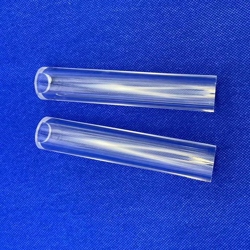
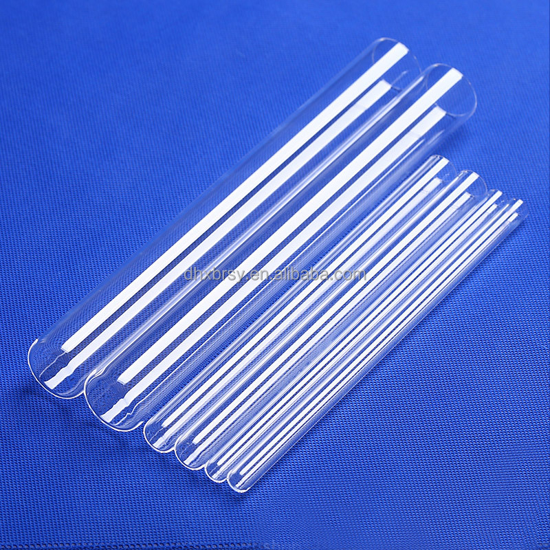
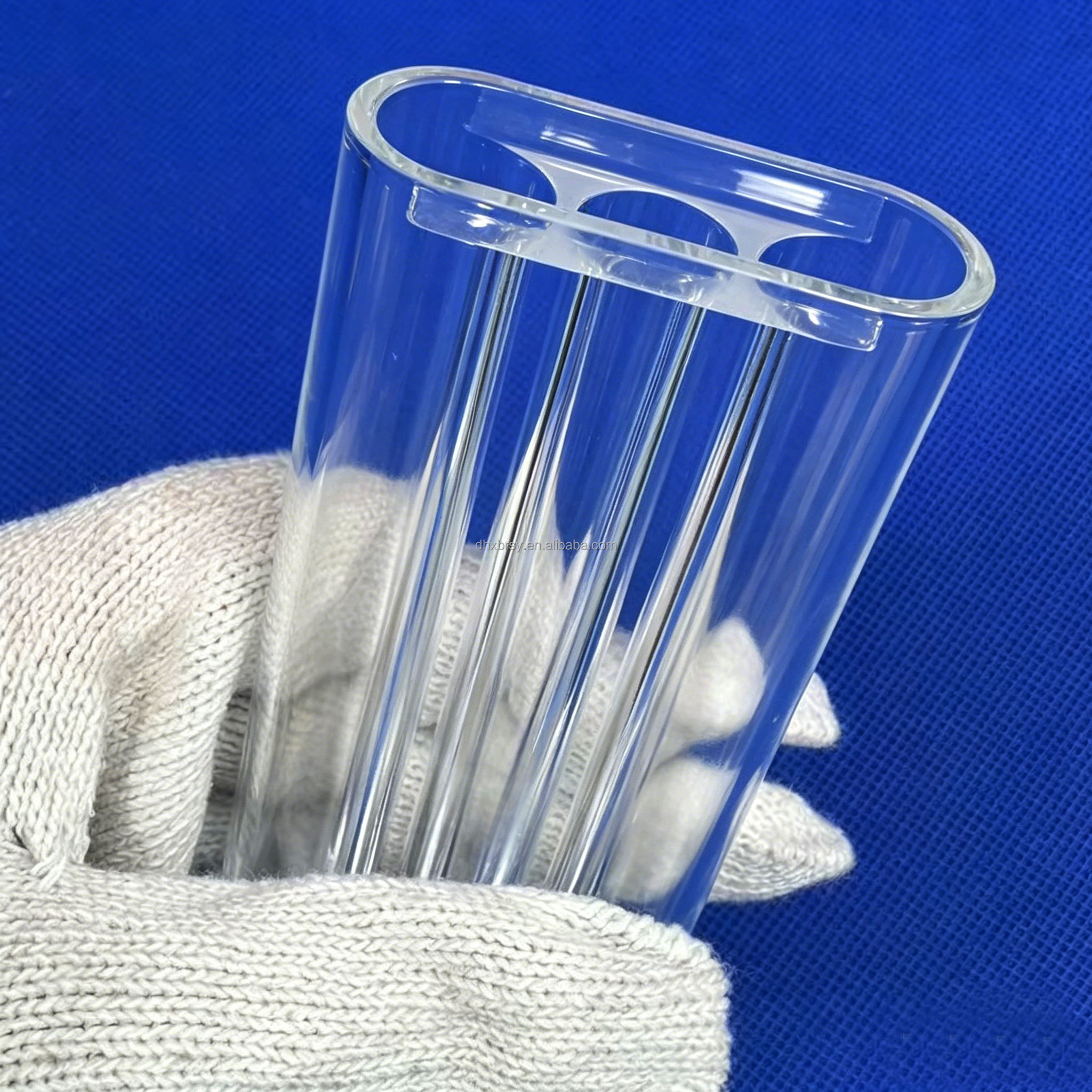
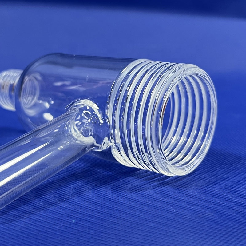
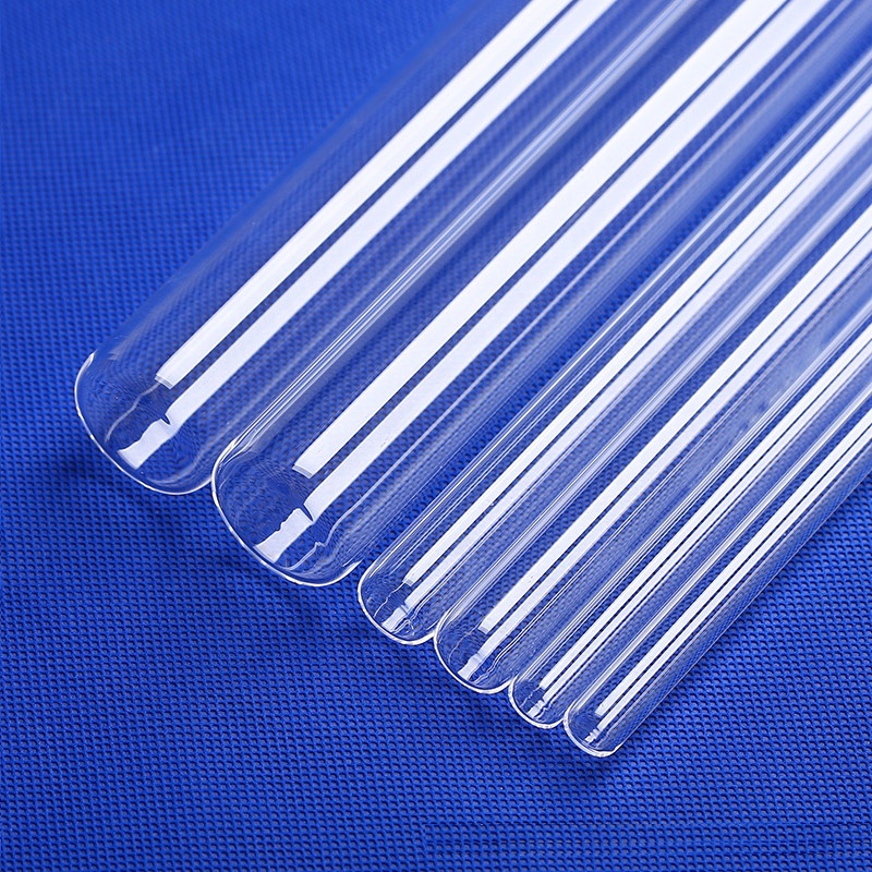
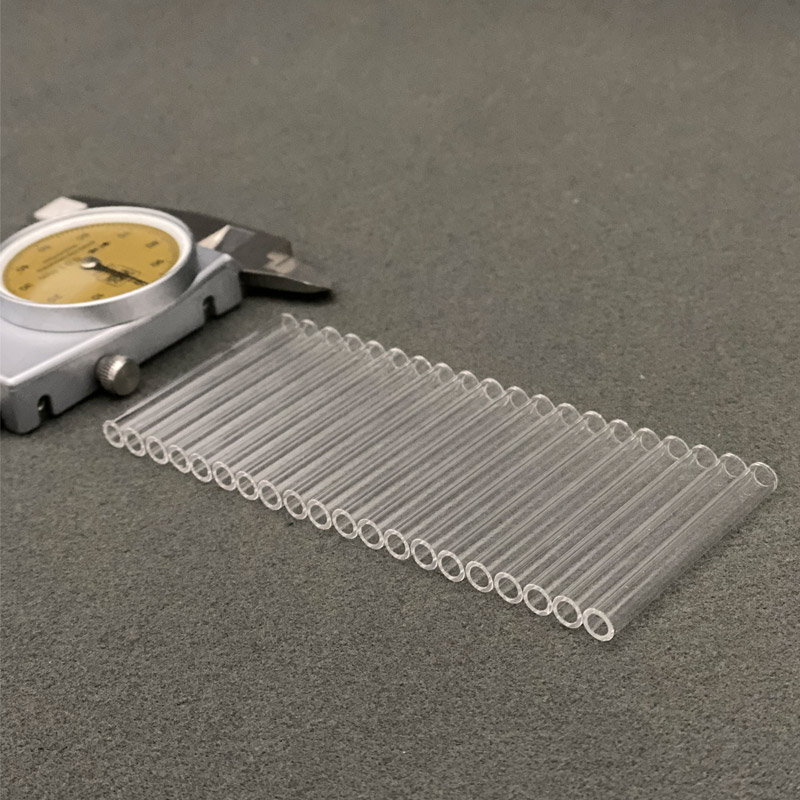
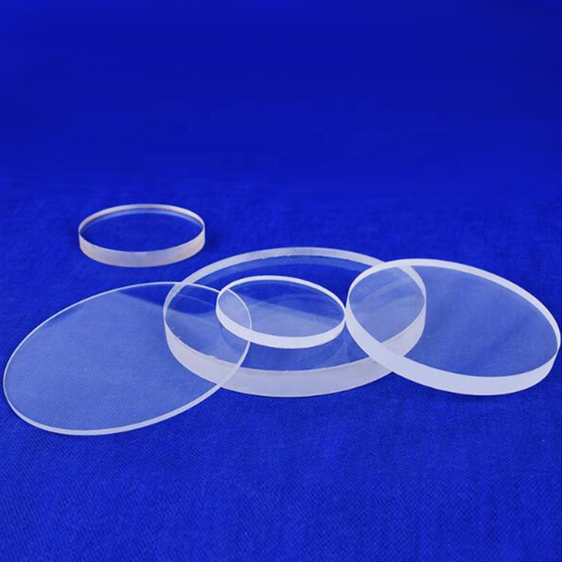
Integrated Vertical Manufacturing & Quality Engineering
Headquartered in Lianyungang, China's premier silicon industrial cluster, Lovri Quartz controls the complete processing line from raw lump quartz crushing and chemical acid-pickling to continuous tube drawing, five-axis CNC shaping, and Class-100 cleanroom packaging.
Purification at Source
By conducting raw quartz sand crushing, magnetic separation, and hydrofluoric/nitric acid leaching in-house, we eliminate trace metal cross-contamination before melting. Metallic impurity levels remain under 15 ppm across bulk runs.
Polarimetric Stress Relief
Micro-cracking during rapid thermal cycling stems from residual annealing strain. 100% of our quartz plates, tubes, and custom apparatus undergo controlled electric annealing followed by transmission polarization stress birefringence analysis.
5-Axis Ultrasonic CNC
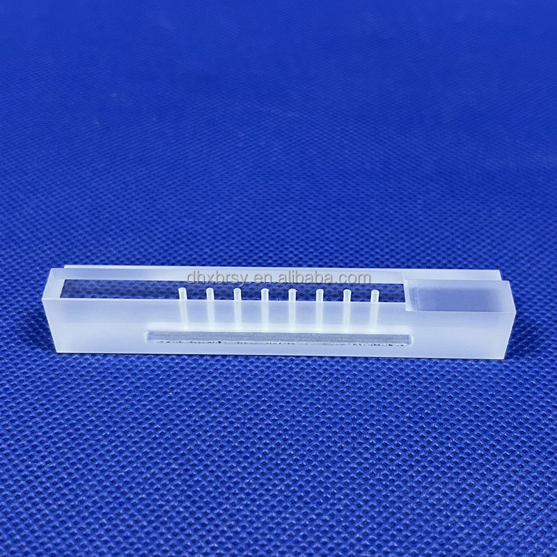
We execute multi-tier blind holes, high-aspect micro-grooves, chamfers, optical flats, and microfluidic channels in fused silica using diamond-tooled ultrasonic CNC machinery, keeping edge-chipping below 20 μm.
Traceable SGS Compliance
Every shipment is accompanied by dimensional inspection protocols, spectral transmittance curves, and RoHS hazardous substance certification. Factory operations are third-party audited under international supplier assurance schemes.
Fused Quartz vs. Synthetic Fused Silica: Substrate Selection Matrix
Selecting the optimal quartz substrate requires balancing deep ultraviolet transparency, hydroxyl [OH-] absorption bands, bubble inclusion classes, and thermal shock thresholds.
| Substrate Grade | Manufacturing Method | Transmission Range | Typical [OH-] Content | Key Industrial Use-Case |
|---|---|---|---|---|
| JGS1 (Synthetic Silica) | SiCl₄ Vapor Deposition | 185 nm – 2500 nm Deep UV | < 5 ppm – 1200 ppm (Grade Dep.) | Excimer laser optics, semiconductor EUV/DUV mask blanks, high-precision prisms |
| JGS2 (Fused Quartz) | Oxy-Hydrogen Flame Fusion | 220 nm – 2500 nm UV / Vis | 150 – 200 ppm | Optical sight windows, UV curing lamp envelopes, spectroscopic cuvettes, furnace viewports |
| JGS3 (Electrically Fused) | Electric Vacuum Melting | 260 nm – 3500 nm Infrared | < 5 ppm (Dry Grade) | Infrared thermal detectors, MWIR windows, wafer diffusion tubes, semiconductor furnace boats |
| Opaque Fused Silica | Gas-Assisted Sintering | Diffuse Reflection (Vis-IR) | < 30 ppm | Thermal shielding, flange gaskets, IR heating spiral surrounds, pyrometry baffles |
Physical, Dielectric, and Mechanical Integrity
Transparent fused silica and fused quartz substrates exhibit a nearly negligible coefficient of thermal expansion (α ≈ 5.5 × 10⁻⁷ /°C from 20°C to 320°C), representing less than one-tenth the thermal expansion rate of borosilicate glass. This structural stability prevents mechanical stress fractures when quartz substrates transition instantly between ambient and 1100°C environments. In semiconductor diffusion, rapid thermal processing (RTP), and metal-organic chemical vapor deposition (MOCVD), this inertness eliminates substrate warping and ensures sub-nanometer thin-film deposition uniformities.
From a dielectric perspective, high-purity quartz substrates possess a dielectric constant (ε) of 3.75 at 1 MHz to 10 GHz and a loss tangent (tan δ) under 0.0001, making them superior low-loss candidates for microwave, millimeter-wave (5G/6G), and RF circuit interposers compared to standard alumina or ceramic substrates.
2025–2030 Trends Shaping Quartz Substrate Sourcing
Procurement directors and component designers are transitioning away from generic quartz stock toward mission-specific chemical and geometric specifications.
Advanced Chip Packaging (CoWoS)
With chiplet architectures demanding ultra-flat carrier wafers, temporary quartz bonding plates with total thickness variations (TTV) < 1 μm are surging in demand. Quartz allows laser debonding throughput unachievable through silicon carriers.
- Laser debonding via high optical transmission
- Elimination of CTE mismatch across thermal cycles
- Ultrasonic hole-drilling for via arrays
CMP Surface Planarization
Optical waveguides, bio-MEMS devices, and AR diffractive gratings require atomic-scale surface finishes. Suppliers must now provide Chemical-Mechanical Polishing (CMP) yielding surface roughness values Ra ≤ 0.3 nm across full 300 mm blanks.
- Scratch-dig specifications exceeding 10-5 standards
- Sub-surface damage (SSD) elimination via double-side CMP
- Interferometric wavefront distortion verification
Reshoring & Dual-Sourced Quartz
Due to geopolitical tensions and supply shocks in raw silicon gas precursors, tier-1 fabs are auditing Chinese source manufacturers directly, vetting vertically integrated players who manage raw mineral acid pickling up to CNC delivery.
- Complete traceability of trace metal parts-per-billion (ppb)
- Consolidated lead times via integrated machine shops
- Custom prototype iterations from low MOQ batches (1–5 pcs)
Frequently Asked Technical & Sourcing Questions
Detailed technical responses addressing tolerances, surface quality, thermal limits, and drawing conversions.
What dimensional tolerances can you hold on custom CNC quartz parts?
For diamond ground and CNC machined profiles, our baseline tolerance is ±0.05 mm. For critical optical substrate applications, including laser window bevels and semiconductor jigs, we consistently hold ±0.005 mm on dimensions, with thickness tolerances under ±0.002 mm and parallelism < 30 arcseconds.
What is the maximum working temperature before devitrification occurs?
Continuous service temperature for our clear fused quartz is 1100°C, with peak short-duration capability up to 1300°C. Devitrification (crystallization back to cristobalite) begins around 1150°C if surfaces encounter alkaline contaminants. Our acid-pickled and cleanroom-handled parts significantly delay devitrification rates.
How do you classify and inspect bubble inclusions in quartz plates?
In accordance with DIN 58927 and ISO 10110 standards, our optical-grade fused silica is certified to Bubble Class 0 (zero bubbles greater than 0.05 mm in critical aperture zones). Routine components are visually inspected under collimated light tables and polariscopes to verify bubble cross-sectional areas.
Can you process substrates based on CAD/STEP drawings?
Yes. Our engineering shop accepts 2D and 3D files in DXF, DWG, STEP, IGES, and PDF formats. Our CAM engineers review all geometries for tool collision, wall aspect ratios, and thermal expansion relief prior to initiating diamond grinding or laser cutting.
How does chemical etching resistance compare against borosilicate?
Fused silica exhibits near-total chemical inertness to hydrochloric, nitric, sulfuric, and organic acids at room and boiling temperatures. Only hydrofluoric acid (HF) and hot concentrated phosphoric acid (>150°C) etch SiO₂ glass. Fused quartz outlasts borosilicate by more than 4× in aggressive acid bath immersion.
What is your export packaging protocol for fragile quartz substrates?
Substrates and tubes are vacuum-sealed in static-shielded cleanroom bags, suspended in custom high-density closed-cell EPE foam cradles, and crated inside fumigated export-grade plywood cases equipped with shock and tilt monitoring indicators.
Submit Your Quartz Substrate Drawings for Engineering Review
Whether you require standard 100 mm – 300 mm fused silica wafer blanks, custom CVD furnace tubes, or micron-precision CNC optofluidic carriers, our engineering team provides rapid DFM feedback, material certification sheets, and volume price breaks within 24 hours.