SEMICONDUCTOR
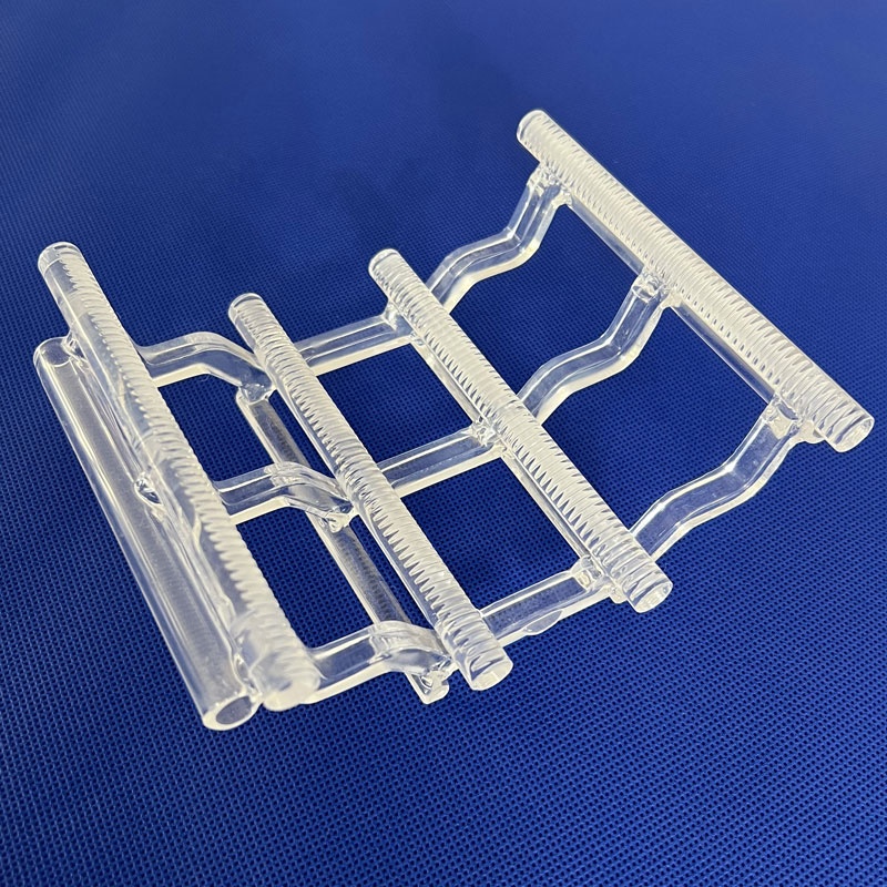
Custom Size High Temperature Fused Quartz Wafer Boat
99.99% SiO₂ material content, zero thermal hysteresis, custom slot pitch design, RoHS certified semiconductor wafer carrier.
Engineered specifically for diffusion furnaces, RF plasma chambers, laser cavities, and photochemical reaction environments. Selected standard prototypes and customized sizes delivered with strict certification.
99.99% SiO₂ material content, zero thermal hysteresis, custom slot pitch design, RoHS certified semiconductor wafer carrier.
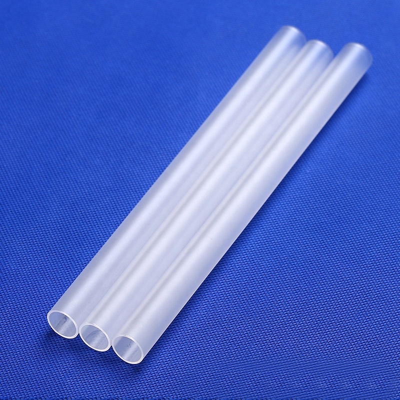
Extreme corrosion resistance, high ozone generation rates, precision fire-polished cut ends for UV sterilization and industrial heating.
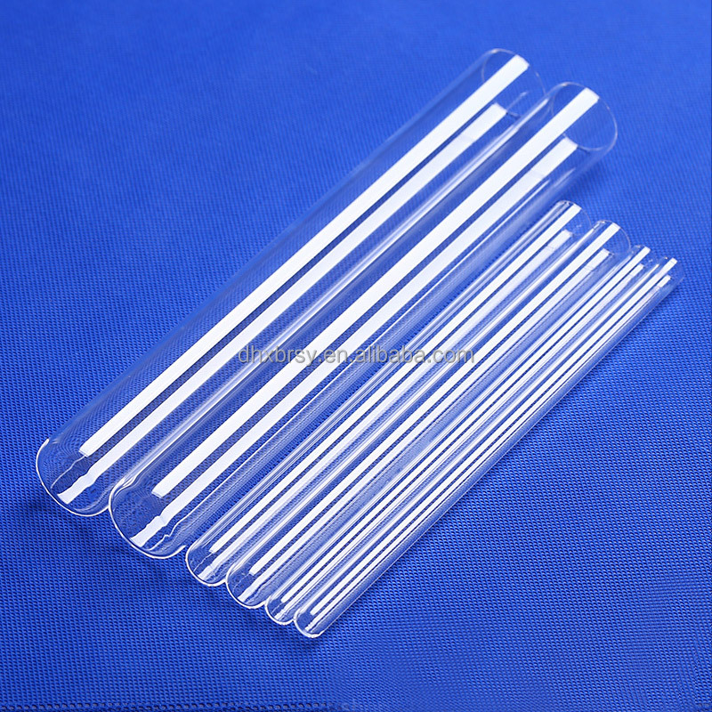
Withstands 1400°C continuous heat ramps, translucent fused quartz wall, engineered for high-pressure laser and plasma reactors.

Deep-UV spectral transmission (185nm-2500nm), bubble-free Grade A surface, annealed at 1200°C for high-energy laser window optics.
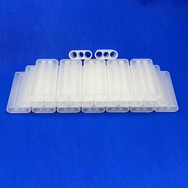
Custom multi-bore fluid dynamic channels, seamless fusion welding, specialized for medical lasers and solid-state pumping chambers.
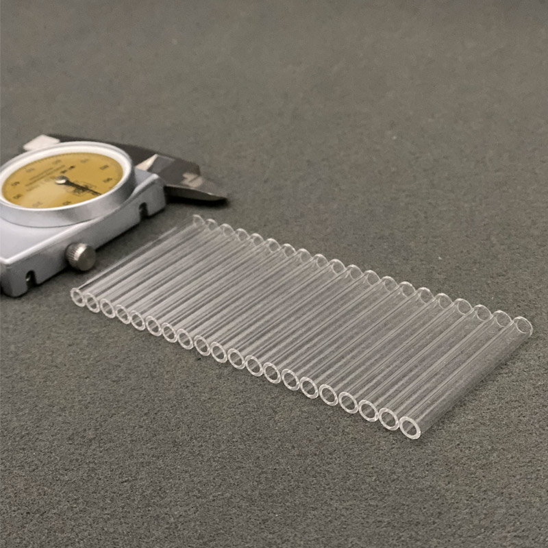
Micro-bore precision bore diameters, 200 Mesh raw silica base, high dielectric breakdown strength for fiber optics and gas chromatography.
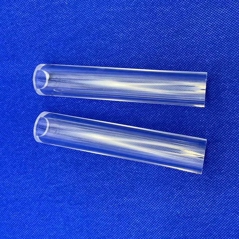
Controlled wall thickness, minimal run-out, optimized for far-infrared heaters, etching exhaust conduits, and ozone quartz reactors.
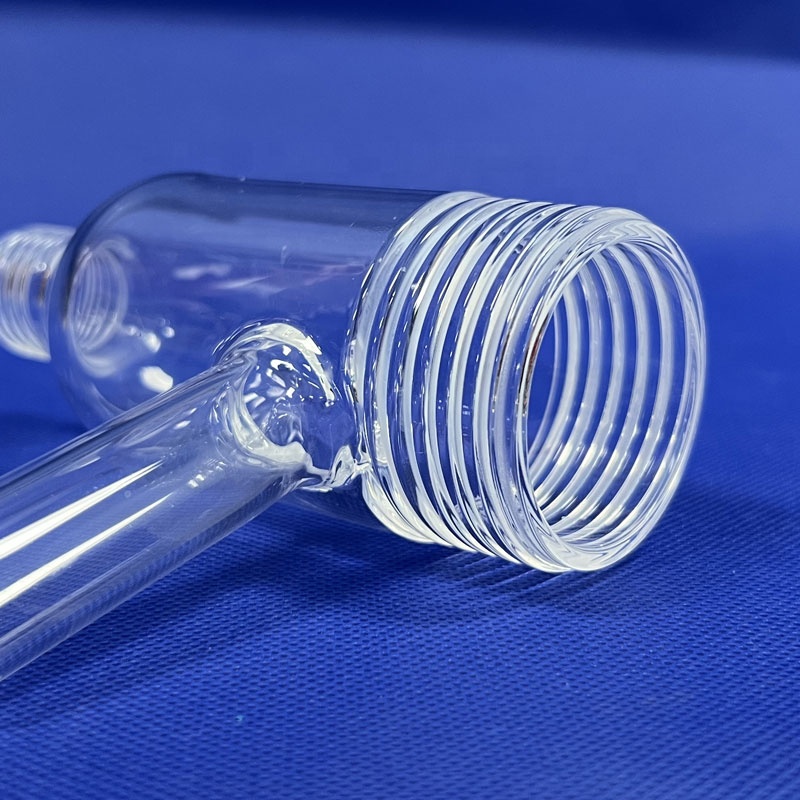
Precision machined quartz threads, ground side arms, vacuum hermetic sealing capability for wet chemical synthesis and thermal CVD testing.
In modern microelectronics, optoelectronics, and micro-electro-mechanical systems (MEMS), fused quartz substrates and fused silica wafers represent essential foundation materials. Unlike standard borosilicate or soda-lime glass, fused silica is composed almost exclusively of amorphous silicon dioxide (SiO₂ ≥ 99.99%). This atomic structural homogeneity delivers an exceptionally low coefficient of thermal expansion (CTE ≈ 5.5 × 10⁻⁷ /°C), enabling components to undergo instantaneous thermal shocks from room temperature to beyond 1100°C without micro-fracturing or volumetric deformation.
For semiconductor fabrication procurement, wafer boats, diffusion tubes, and sacrificial monitoring wafers must maintain ultra-low trace alkali metallic impurities (such as Sodium, Potassium, and Lithium < 0.1 ppm). In elevated furnace environments (>1000°C), metallic contaminants easily mobilize and drift through the crystal lattice of silicon wafers, causing gate oxide degradation and deep-level recombination defects. At Lovri Quartz Products Co., Ltd., our raw sand beneficiation integrates hydrofluoric acid pickling, multi-stage flotation, and magnetic separation to safeguard our products against metal contamination at the atomic boundary.
| Material Standard | Refractive Index (nd) | Transmission Band | OH- Content Level | Primary Industrial Applications |
|---|---|---|---|---|
| JGS1 (Synthetic Silica) | 1.4585 | 185 nm – 2,500 nm (Deep UV) | < 5 ppm to 1200 ppm | Excimer lasers, lithography steppers, photolithography mask blanks |
| JGS2 (Fused Quartz) | 1.4584 | 220 nm – 2,500 nm (Standard Optical) | < 30 ppm | High-temperature viewports, plasma etching windows, UV disinfection tubes |
| JGS3 (Infrared Fused Quartz) | 1.4580 | 260 nm – 3,500 nm (Full IR) | < 5 ppm (Water-Free) | Infrared thermography windows, thermal sensors, IR heaters |
| Opaque Fused Silica | N/A (Scattering) | Diffuse thermal reflection | Varied | Heat diffusion barriers, flange heat insulators, furnace baffles |
Procurement directors and strategic sourcing leads are realigning their supply chain matrices in response to generational changes across advanced nodes (3nm/2nm GAA architectures), Third-Generation Semiconductors (SiC/GaN), and large-scale PV cell efficiency transitions. Key procurement trends shaping supplier selection include:
As wafer-to-wafer direct bonding and EUV mask blanks expand, wafer buyers require Chemical-Mechanical Planarization (CMP) capable of reducing surface microroughness below 3 angstroms, coupled with Total Thickness Variation (TTV) < 1.5 μm.
Global FABs now demand complete traceability from raw high-purity quartz (HPQ) granulate through to finished machined wafer boats. Fabricators must ensure zero cross-contamination throughout acid leaching, hot drawing, and furnace annealing.
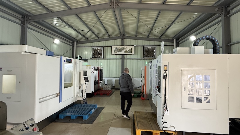
To reduce thermal-stress failure points caused by traditional torch-welded joints, equipment makers are shifting toward single-piece 5-axis ultrasonic CNC milling for quartz showerheads, wafer boats, and vacuum chamber liners.
Headquartered in Tuofeng Industrial Park, Lianyungang, Jiangsu — China's central fused quartz manufacturing cluster. Lovri integrates vertical supply chains from raw silica processing to precision inspection.
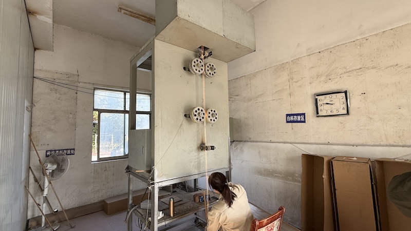
Operating across 14,271 m² of floor space, we control raw quartz pulverization, multi-stage acid pickling, automated tube drawing, and precision annealing directly on-site to ensure full cost and lead-time control.
Our workshop, production capacities, quality testing equipment, and export workflows have undergone comprehensive onsite qualification by SGS Group, providing genuine accountability for global engineering projects.
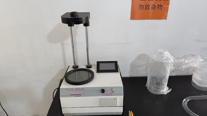
Latent thermal stress causes cracking during high-temperature furnace cycling. We inspect every batch using polarization stress analyzers to guarantee uniform structural relaxation prior to shipment.
From 1-piece pilot development runs to continuous monthly wafer boat replenishment programs, our rapid-response CAD/CAM engineering team accepts drawings in PDF, DWG, DXF, or STEP formats.
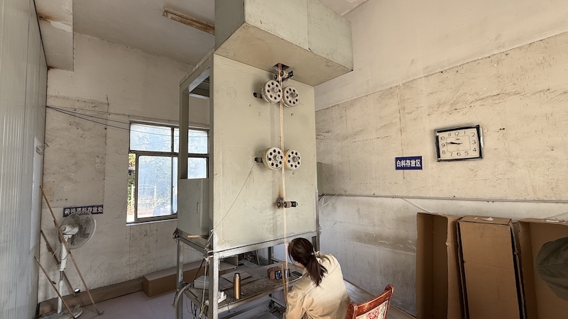
Key considerations covering quality metrics, tolerance control, packaging parameters, and export certification.
Upload your mechanical drawings (PDF, DWG, DXF, or STEP) along with your working temperature parameters, optical transmission targets, and required volume. Our technical engineering specialists will evaluate your requirements and provide a direct quotation within 24 hours.