SiO₂ ≥ 99.99%
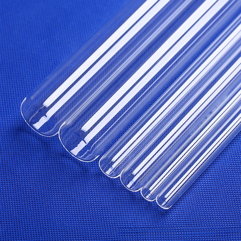
Customized Clear Quartz Glass Tube Fused Silica One End Closed
Semiconductor tube profile • Annealed up to 1200°C • Flat or round bottom custom geometries for high-temp processing.
From single-end closed furnace tubes to triple-bore laser cavity flow sleeves and high-transmittance optical plates, our precision quartz components undergo 100% polarization stress testing and stringent dimensional metrology.
Semiconductor tube profile • Annealed up to 1200°C • Flat or round bottom custom geometries for high-temp processing.
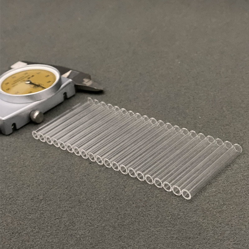
200 Mesh (75μm) precision • 99.99% pure silica • Stress-relieved at 1200°C for high-energy medical and industrial laser systems.
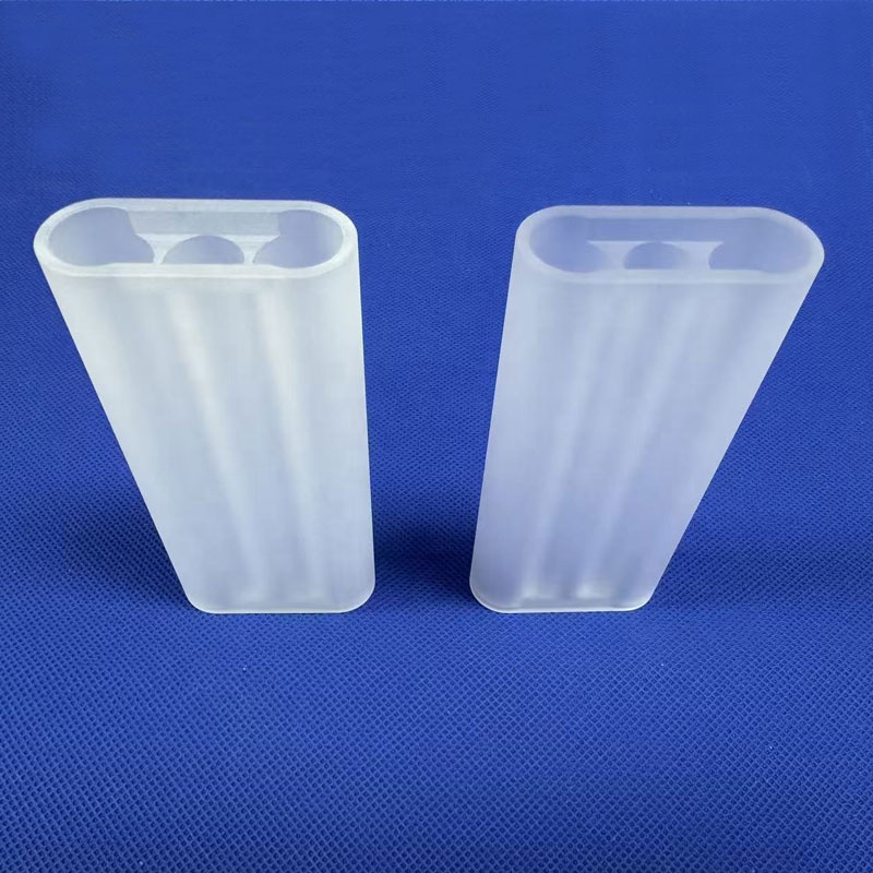
Engineered for GentleYag/GentleMax aesthetic lasers • Uniform cooling cavity geometry • High thermal-shock tolerance.
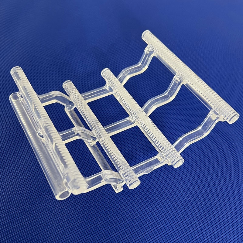
Micro-slotted wafer carrier • Ultra-low thermal expansion (5.5×10⁻⁷/°C) • Inert to oxidation and diffusion environments.
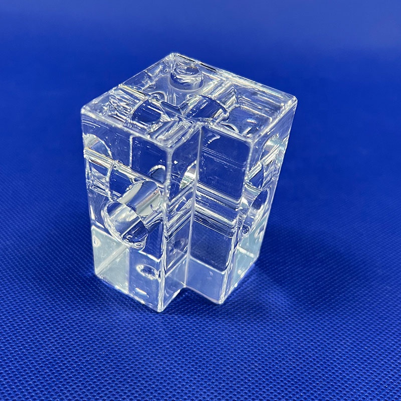
Annealed at 1200°C • RoHS certified • Specially formatted for analytical microfluidics, sight glasses, and flow cytometry.
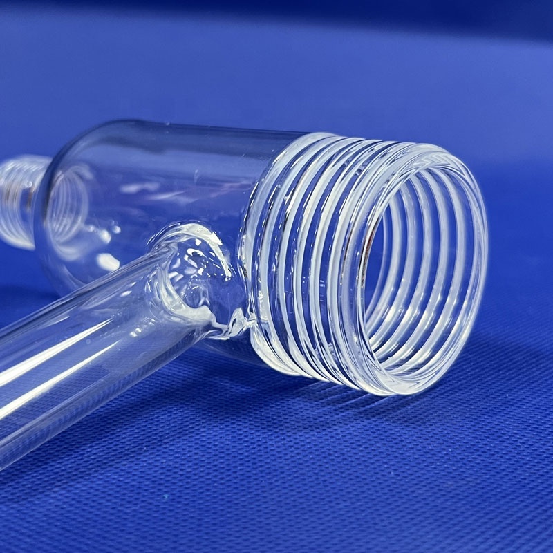
Precision screw threads • Optical clarity • Leak-tight quartz-to-metal and PTFE adaptability for high-purity synthesis.
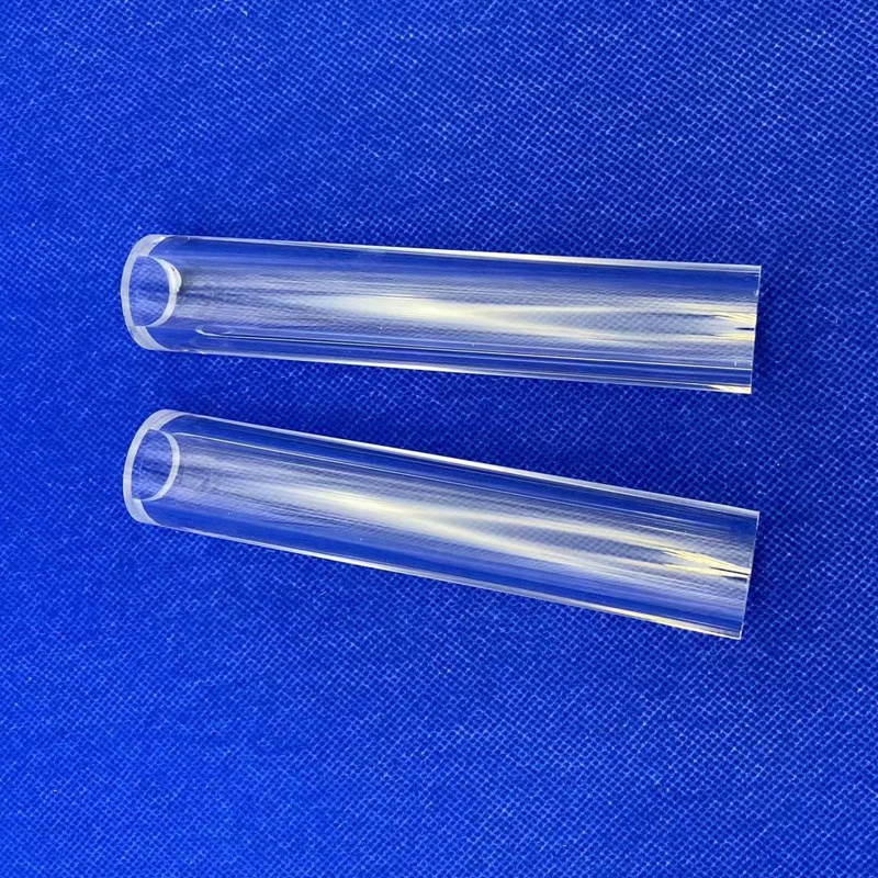
Custom bending, fire-polishing, and welding • Dielectric strength for corona discharge • High thermal radiation efficiency.
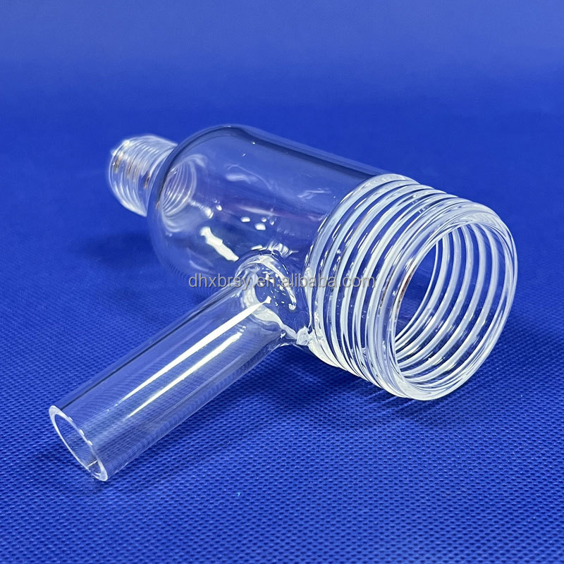
Superior optical surface finish • Acid/alkali corrosion resistance • Machined inner/outer threads to tight DIN/ISO tolerances.
In high-precision optical, semiconductor, and optoelectronic engineering, a fused silica window serves as an indispensable transmissive interface that isolates varying pressure regimes, elevated thermal zones, or corrosive gaseous environments while delivering distortion-free optical transmission. Understanding the crystallographic synthesis and atomic purity differences among synthetic fused silica, flame-fused natural quartz, and electrically fused silica is vital for optical procurement engineers striving to eliminate laser-induced damage, wave-front aberration, and chromatic distortion.
Synthesized via high-purity SiCl₄ chemical vapor deposition. Features virtually zero metallic impurities, absence of bubble inclusions (ISO 10110 Class 0), and unmatched transmission down to 185 nm in the Deep-UV (DUV) band.
Produced by flame fusion of high-purity natural silica sand. Offers excellent transmission across 220 nm to 2500 nm, providing a cost-optimized solution for UV-Vis inspection windows, sight glasses, and photolithography stages.
Electrically fused under vacuum conditions to suppress hydroxyl (OH⁻) content below 5 ppm. Eliminates the prominent 2.73 μm absorption band, unlocking superior infrared clarity up to 3500 nm for thermal imaging viewports.
| Physical / Optical Parameter | JGS1 (Synthetic Fused Silica) | JGS2 (Optical Fused Quartz) | JGS3 (Infrared Fused Quartz) | Borosilicate Float Glass | Single-Crystal Sapphire (Al₂O₃) |
|---|---|---|---|---|---|
| Spectral Transmission Window | 185 nm – 2500 nm (DUV to NIR) | 220 nm – 2500 nm (UV to NIR) | 260 nm – 3500 nm (NIR to Mid-IR) | 350 nm – 2000 nm (Visible only) | 150 nm – 5500 nm (Broadband) |
| Hydroxyl [OH⁻] Content | 1200 – 1500 ppm (High OH) | 150 – 200 ppm (Standard) | < 5 ppm (Water-Free) | Variable / Non-Optical | < 1 ppm (Anhydrous) |
| Coefficient of Thermal Expansion (CTE) | 5.5 × 10⁻⁷ / °C (20–300°C) | 5.5 × 10⁻⁷ / °C | 5.5 × 10⁻⁷ / °C | 32.5 × 10⁻⁷ / °C (6× higher) | 58 × 10⁻⁷ / °C (10× higher) |
| Thermal Shock Resistance (ΔT) | > 1100°C to Ice Water quench | > 1000°C quench | > 1000°C quench | ≈ 150°C maximum | ≈ 300°C (Risk of cleavage) |
| Continuous Working Temperature | 1100°C (Anneal point: 1215°C) | 1100°C (Strain point: 1120°C) | 1150°C | 450°C | 1600°C |
| Laser Damage Threshold (LIDT @ 1064nm, 10ns) | > 25 J/cm² (Super-polished) | ≈ 15 J/cm² | ≈ 18 J/cm² | < 3 J/cm² (Prone to ablation) | > 20 J/cm² |
| Internal Stress Birefringence | ≤ 2 – 5 nm/cm (Optical Class 1) | ≤ 10 nm/cm | ≤ 10 nm/cm | Not specified (> 30 nm/cm) | Birefringent (Uniaxial Crystal) |
The international supply ecosystem for precision quartz glass is undergoing a seismic realignment driven by semiconductor miniaturization, laser machining power scaling, and aerospace telemetry hardening. Supply chain directors and technical procurement managers are shifting away from transactional broker sourcing toward direct tier-1 source manufacturing partnerships characterized by vertical purity verification, guaranteed traceability, and custom dimensional agility.
Advanced fabs operating at ≤3nm nodes require sub-ppb metallic impurity limits. Procurement workflows increasingly stipulate source-level purity certificates (ICP-MS testing) starting from natural quartz lump pickling up to wafer boat annealing. Middlemen and distributors are bypassed in favor of vertically integrated factories that control chemical refinement in-house.
With industrial fiber lasers routinely eclipsing 12kW to 30kW, standard quartz protective windows experience catastrophic thermal lensing and catastrophic bulk failure. Buyers are requiring synthetic JGS1 substrates polished to surface roughness Ra < 0.5 nm with dual-sided ion-assisted e-beam dielectric anti-reflective (AR) coatings offering absorption < 5 ppm.
Procurement contracts no longer accept generic visual clarity assertions. Quantitative polariscope inspections, interferometer surface wave-front documentation (λ/10 to λ/20 PV), and SGS onsite physical facility accreditations are baseline prerequisites for defense, analytical biomedical, and space payload optical assemblies.
To address increasingly hostile processing regimes—including fluorine plasma etching in atomic layer deposition (ALD), extreme cryogenic-to-high-temperature cycling, and vacuum ultraviolet (VUV) irradiation—the manufacturing processes governing fused silica windows have evolved dramatically beyond traditional loose-abrasive grinding and torch sealing.
Sub-aperture deterministic polishing eliminates subsurface damage (SSD), achieving surface roughness Ra < 0.2 nm (Super-Polishing). This elevates laser damage thresholds (LIDT) exponentially for next-generation petawatt lasers.
Applying nitrogen-doped silicon oxynitride or fluorinated interfacial barriers onto quartz furnace viewports to prevent aggressive fluorine radical and halite etching during semiconductor PECVD clean cycles.
Diamond micro-tooling coupled with high-frequency ultrasonic excitation allows micro-drilling, complex blind step slots, and miniature internal threading in brittle quartz without edge chipping or micro-fracturing.
Situated in Lianyungang, Jiangsu—the epicenter of high-purity crystalline silica refinement in China—Lovri Quartz operates a modernized, SGS onsite-assessed 14,271 m² production facility. We unite raw mineral crushing, high-temperature furnace tube drawing, precision optical annealing, and multi-axis CNC machining under one roof, guaranteeing complete quality oversight, uncompromised material traceability, and competitive direct-factory cost structures.
High-grade quartz lumps pulverized, re-screened to 200 mesh (75μm), and triple acid-pickled to reach ≥ 99.99% SiO₂ purity.
Continuous tube drawing, electric-arc crucible ingot fusion, and precision hot glassblowing for large-bore furnace tubes and flanges.
1200°C controlled soaking and gradual cool-down schedules in computerized furnaces to extinguish internal stress and molecular strain.
100% batch validation on high-sensitivity polarization stress testers ensuring optical class 1 retardation (≤ 5 nm/cm).
High-precision diamond grinding, step profiling, drilling, chamfering, and internal/external thread cutting to ±0.005 mm tolerances.
Double-sided planetary pitch polishing achieving surface roughness Ra < 0.5 nm and scratch-dig specifications of 20-10 or 10-5.
Seamless quartz-to-quartz welding, vacuum evacuation, and side-arm port fusion executed by master scientific glassblowers.
Ultrasonic deionized water cleaning, anti-static vacuum wrapping, and reinforced wooden crating engineered for zero-breakage international transit.
Clear, technically rigorous answers to the critical engineering and commercial questions raised by optical designers, semiconductor equipment builders, and supply managers.
Whether you require prototype DUV synthetic fused silica windows, large-diameter CVD reaction cylinders, slotted semiconductor wafer boats, or high-temperature sight glasses, our optical engineers will evaluate your drawings, recommend optimal quartz grades, and return a factory-direct quotation within 24 hours.