Engineered Quartz Substrates & Custom Apparatus
Manufactured from natural and synthetic silica crystals under strict polarization-stress testing. Precision CNC ground, flame polished, and vacuum annealed to meet demanding cleanroom and R&D standards across Western Sweden.
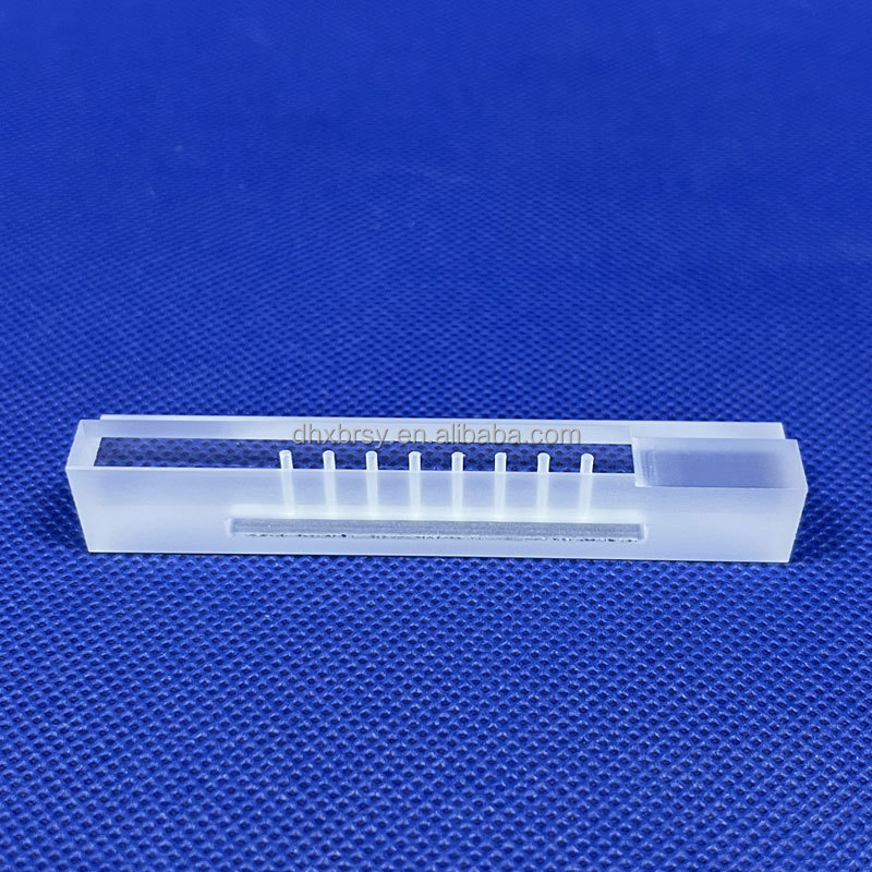
High Purity Fused Quartz V-Groove Fixture Fiber Array Holder
Pitch accuracy ±0.5 μm, 99.99% SiO&sub2;, designed for fiber coupling, optical communication transceivers, and quantum computing interconnects.
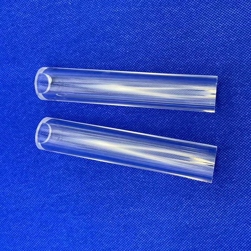
High Precision Clear Fused Silica Quartz Glass Tube
Tight OD/ID tolerances, ozone generator compatible, excellent thermal shock resistance up to 1200 °C for industrial pyrolysis and heaters.
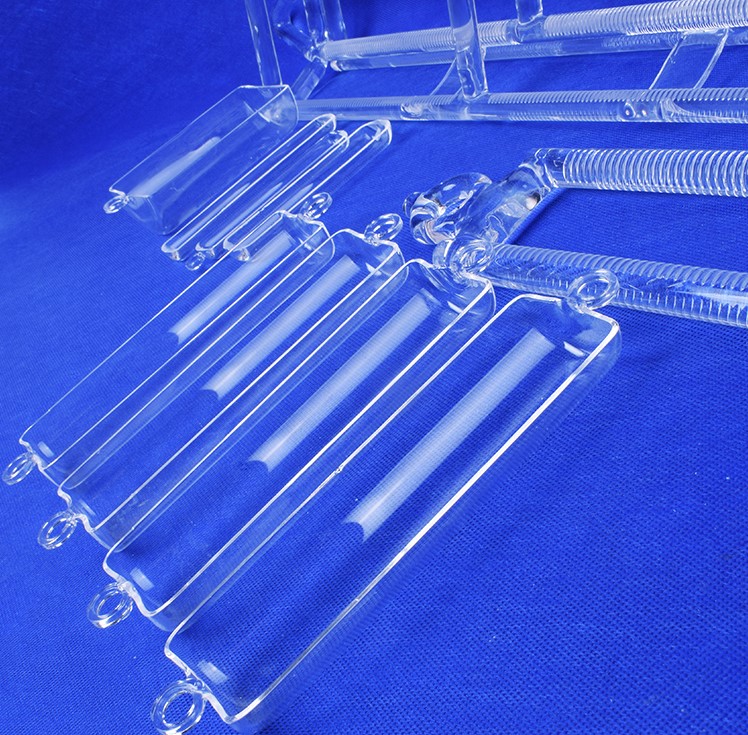
Fused Quartz Wafer Boats (SiO₂ 99.99%) for Solar & Semi
Acid-cleaned, custom slot pitch for 2″ to 12″ wafers, high chemical resistance against HF acid blends and ultra-low thermal sagging.
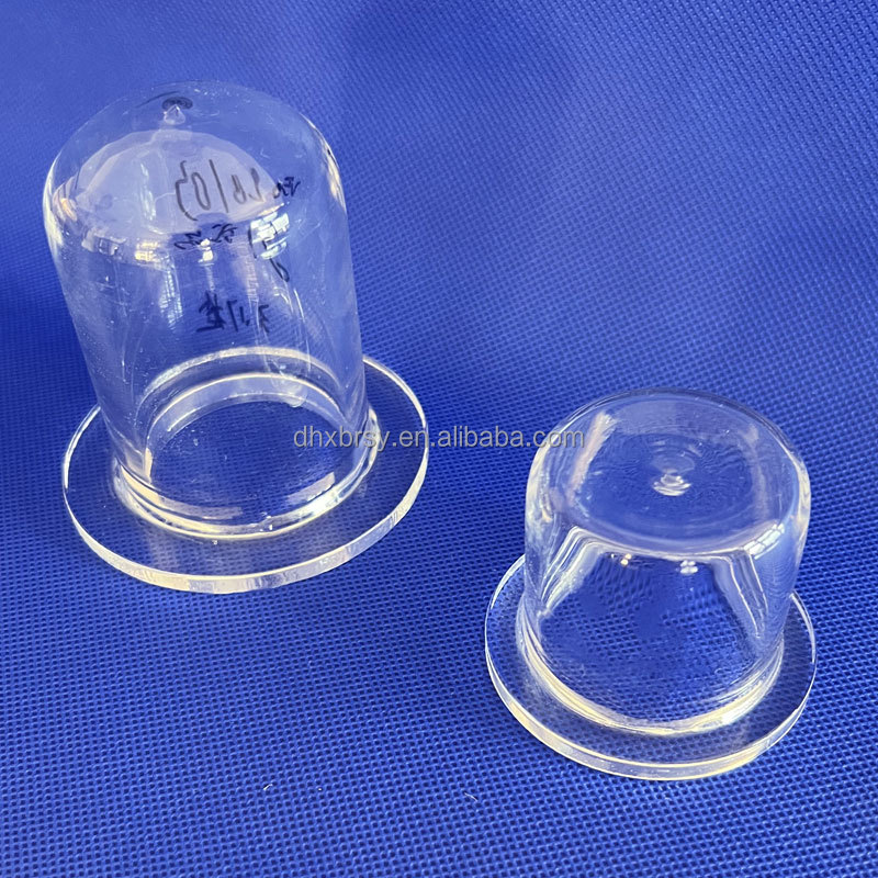
High Transmittance Quartz PV Cell Sintering Furnace Muffle
RoHS certified, near-zero hydroxyl (OH) options for extreme infrared pass-through, robust against continuous thermal gradients.
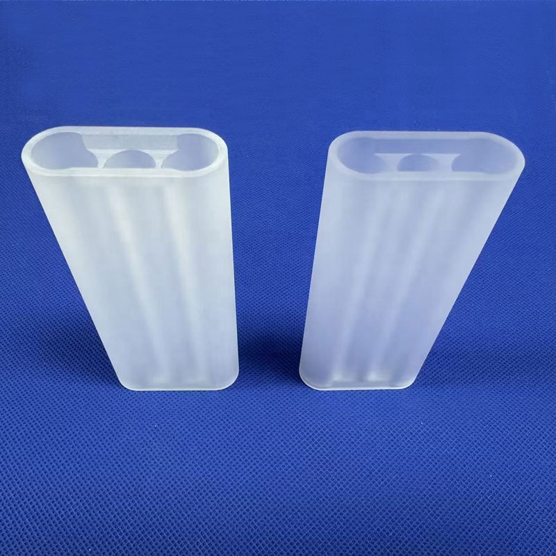
High Precision Triple Bore Quartz Laser Cavity Flow Tube
Precision fused flow cell for solid-state and medical laser cooling. High UV-VIS transmittance, tight internal parallelism, and zero bubble inclusion.
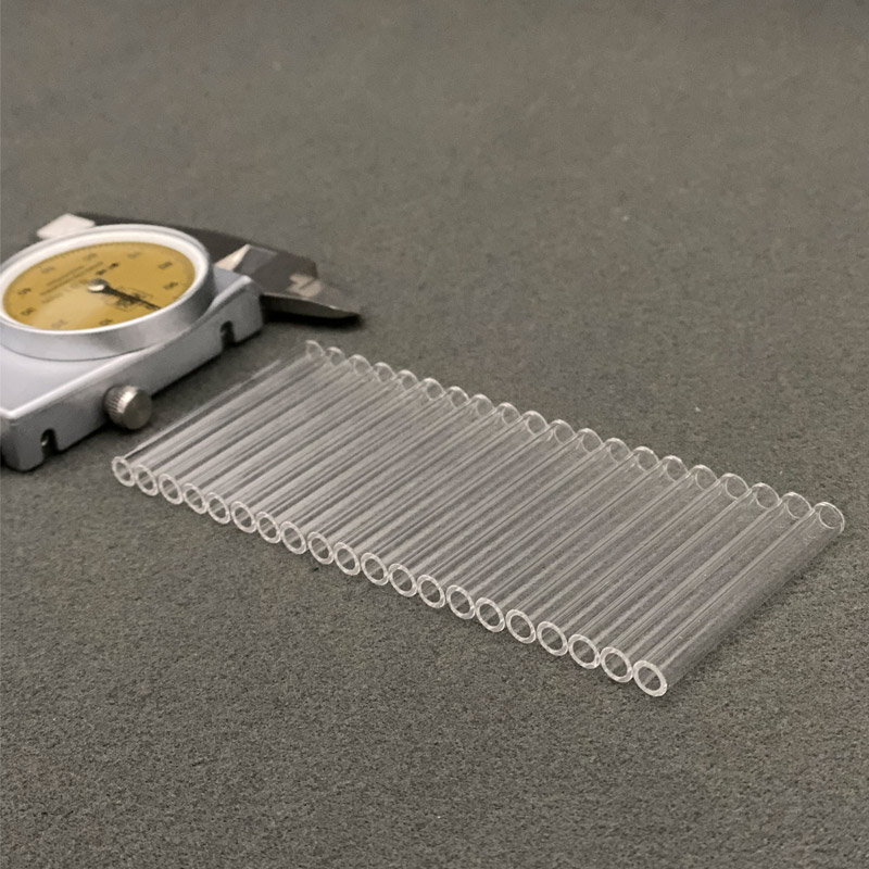
Fused Quartz Capillary Tube (Annealed 1200°C) for Laser
Precision inner bore, vacuum degassed, RoHS compliant. Engineered for analytical gas chromatography, laser guides, and bio-sensors.
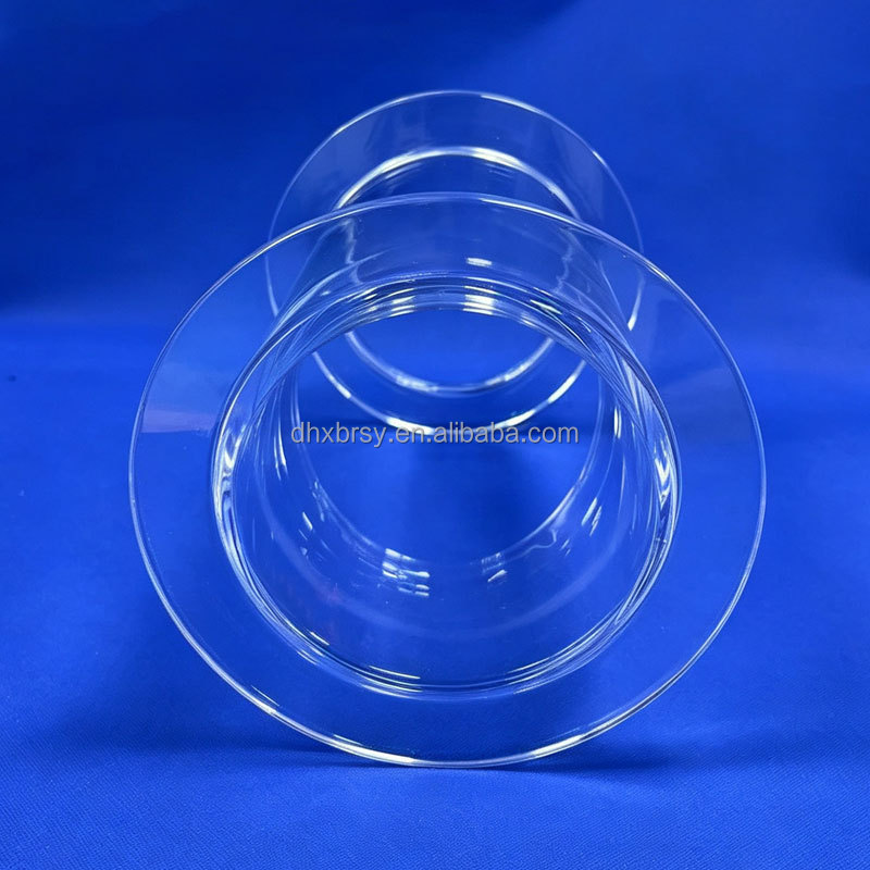
Double-Flanged Transparent Quartz Reaction Cylinder
Optical-grade polished sealing faces, CNC ground bolt holes, suitable for plasma etch, ALD, and semiconductor CVD processing tools.
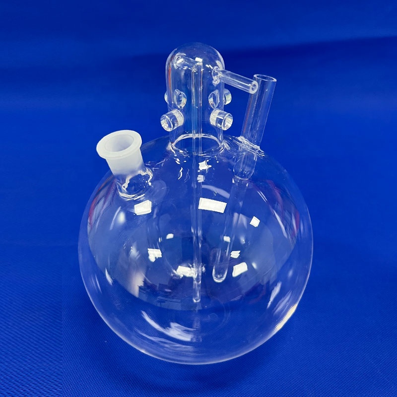
Custom High-Purity SiO₂ Glass Laser Chemical Reactor
Seamlessly welded branched joints, threaded ports, pressure tested for photochemical synthesis, laser catalysis, and analytical flow cells.
Fused Silica Substrate Material Science & Optical Characterization
For procurement directors, cleanroom principal investigators, and optical designers in Gothenburg: understand transmission windows, OH content, and thermal-expansion dynamics to select the optimal quartz substrate.
Optical Quartz Grade Matrix: JGS1 vs. JGS2 vs. JGS3
Selecting the proper grade is vital to avoid solarization, phase shift, or unexpected dielectric attenuation in high-frequency microwave and deep-UV photonic circuits. Our manufacturing facility in Lianyungang refines crystal quartz and synthetic precursors under vacuum furnace environments, delivering distinct transmission bands:
| Grade Standard | Raw Material Precursor | Transmission Spectrum | Hydroxyl (OH⁻) Level | Primary Gothenburg Application |
|---|---|---|---|---|
| JGS1 (Corning 7980 Equiv.) | Synthetic SiCl₄ Vapor Deposition | 185 nm – 2,500 nm (Deep UV to VIS) | < 5 ppm – 1,200 ppm (Grade specific) | Chalmers Nanofabrication, DUV Lithography, Excimer Optics |
| JGS2 (Heraeus Herasil Equiv.) | Flame Fused Natural Silica Sand | 220 nm – 2,500 nm (Near UV to VIS) | 150 ppm – 300 ppm | Automotive LiDAR Windows, Spectroscopy, Sight Glasses |
| JGS3 (Suprasil 300 Equiv.) | Electrically Fused Natural Quartz | 260 nm – 3,500 nm (VIS to Mid-IR) | < 5 ppm (Water-free IR) | Thermal Imaging Sensors, IR Heating Tubes, Laser Cavities |
| Opaque Fused Silica | Micronized Natural Silica Grain | Diffuse / Opaque Scattering | Standard Trace | Furnace Heat Shields, High-Thermal Sintering Insulators |
Beyond transmission, thermal behavior governs substrate survivability in extreme environments. Transparent fused silica exhibits an exceptionally low thermal expansion coefficient (α ≈ 5.5 × 10⁻⁷ /°C from 20°C to 320°C), outperforming borosilicate and alumina substrates by an order of magnitude. This minimizes wave-front distortion under laser irradiation and prevents cracking during rapid thermal processing (RTP).
Physical, Thermal & Dielectric Specifications
All substrate slabs, wafers, and CNC apparatus undergo double-sided planetary chemo-mechanical polishing (CMP) to achieve sub-nanometer surface roughness (Ra ≤ 0.5 nm / 5 Å), providing clean surface states for epitaxial thin-film deposition and bonding.
| Physical Property | Tested Metric | Standard Value | Engineering Significance |
|---|---|---|---|
| Purity (SiO₂) | ICP-MS Spectrometry | ≥ 99.99% – 99.999% | Eliminates heavy metal contamination in cleanrooms |
| Density | Archimedes Immersion | 2.20 ± 0.01 g/cm³ | Lightweight rigidity for structural aerospace optics |
| Dielectric Constant (ε) | 1 MHz @ 25°C | 3.75 – 3.80 | Ultra-low RF loss for high-speed radar and 5G antennas |
| Dielectric Loss Tangent (tan δ) | 10 GHz @ 25°C | < 0.0001 | Critical for Millimeter-wave & Terahertz waveguide windows |
| Annealing Point | ASTM C598 | 1,150 °C – 1,215 °C | Relieves molecular birefringence via polarization testing |
| Softening Point | ASTM C338 | 1,680 °C – 1,730 °C | Thermal stability far above standard borosilicate limits |
| Surface Flatness | Zygo Laser Interferometer | λ/4 to λ/10 per inch | Prevents fringe distortion in interferometric sensors |
Empowering Gothenburg’s High-Tech & Industrial Frontiers
Gothenburg (Göteborg) has transformed from Scandinavia’s maritime trade capital into an elite hub for nanosciences, vehicle electrification, biopharma, and microwave electronics. Our custom quartz substrates integrate directly into these supply chains.
Chalmers & Microtechnology Cleanrooms
Operating within Chalmers University of Technology's Nanofabrication Laboratory and MC2 (Department of Microtechnology and Nanoscience), researchers require ultra-flat, high-purity synthetic quartz wafer discs.
- E-beam lithography mask blanks with chromium coating
- Quantum qubit superconducting circuit base substrates
- In-situ plasma etch quartz shields and diffusion boats
Automotive LiDAR & Sensor Testing
Surrounding Lindholmen Science Park and Torslanda’s mobility clusters, automotive engineers develop next-generation autonomous sensor suites, requiring durable optical windows.
- Near-IR transparent 905 nm and 1550 nm protective covers
- Anti-abrasion quartz plates for road-test optical chambers
- Precision optical prisms for beam-steering alignment
Life Science & BioVentureHub Systems
At AstraZeneca’s BioVentureHub in Mölndal and Sahlgrenska Science Park, bio-analytical instruments depend on fluorescence-free optical quartz.
- High-precision UV flow-through spectrometry cells
- Capillary electrophoresis tubes and 96-well quartz plates
- Chemical synthesis autoclaves with quartz sight windows
Gothenburg Procurement Trends: Reshoring, Traceability & Carbon Auditing
How technology leaders across Västra Götaland balance global supply chains with strict Swedish sustainability mandates and Tier-1 quality certifications.
Procurement managers in Sweden increasingly prioritize total cost of ownership (TCO) over raw component unit costs. Fragile, high-tolerance components like fused quartz substrates present unique challenges in international logistics:
1. Direct Factory Integration via Port of Gothenburg (Göteborgs Hamn): By sourcing directly from our integrated plant in Lianyungang, buyers eliminate middlemen, gaining full batch transparency. Heavy furnace tubes and large-diameter quartz reactors can be shipped via multimodal container freight into the Port of Gothenburg—the largest port in the Nordic region—while expedited R&D wafers and prototypes are air-shipped to Gothenburg Landvetter Airport (GOT) within 3 to 5 business days.
2. Material Compliance (RoHS, REACH & Conflict Minerals): Swedish environmental legislation mandates exhaustive documentation. Our fused silica products are certified fully compliant with EU RoHS and REACH regulations, accompanied by SGS chemical assay reports verifying non-detectable levels of lead, mercury, cadmium, and polybrominated biphenyls.
3. Stress-Relief Verification: Nordic winters and rapid cleanroom temperature cycles can trigger catastrophic spontaneous fracture in improperly annealed quartz. Our proprietary polarization stress testing protocols eliminate micro-birefringence before precision diamond dicing and grinding.
Why Gothenburg Tech Leaders Choose Lovri Quartz
Vertical control from raw silica rock to multi-axis CNC micro-machining ensures consistency, speed, and drawing accuracy.
14,271 m² Dedicated Facility
Onsite assessed and verified by SGS Group. Houses 12 distinct production workshops, including crushing, tube drawing, vacuum forming, and precision grinding.
Complete Raw Material Line
We process raw silica lump through acid pickling, calcining, and thermal melting, guaranteeing base purity of 99.99% SiO₂ and avoiding second-hand material variability.
Full Polarization Stress Audits
Every single batch passes 1200°C annealing cycles and is inspected under strain viewing instruments to prevent internal micro-fractures in Gothenburg laboratories.
Export-Grade Clean Packaging
Components are ultrasonic-cleaned, vacuum sealed in dual anti-static PE bags inside class 10,000 clean environments, and suspended in shock-proof custom wooden crates.
Frequently Asked Questions by Swedish Buyers
Key considerations regarding customs, delivery times, technical drawing formats, and cleanroom readiness.
What is the typical transit lead time to Gothenburg facilities?
For rapid prototypes, custom optical windows, and CNC laser flow tubes, air courier shipments (via DHL/FedEx/UPS Express) clear customs at Landvetter Airport (GOT) and reach Gothenburg locations in 4–6 business days. Volume batches, bulk quartz tubes, and furnace muffles ship by sea directly to Port of Gothenburg within approximately 26–32 days.
How do you handle import duties, VAT, and Swedish customs clearance?
We supply full commercial invoices, packing lists with clear HS Code classifications (typically 7002.31 or 7002.32 for fused quartz apparatus and tubes), and Certificates of Origin. Swedish companies registered with Tullverket (Swedish Customs) can easily handle their standard import VAT reverse-charge and EU trade compliance.
What CAD formats and dimensional tolerances are supported?
Our CNC 5-axis machining stations accept standard CAD formats including STEP (.stp), IGES (.igs), DXF, and DWG, along with toleranced engineering PDFs. Standard linear tolerances are held to ±0.05 mm, with precision ground optical surfaces achievable down to ±0.002 mm and surface flatness to λ/10.
How are brittle quartz substrates protected during international transit?
We employ a multi-barrier export packaging system: parts are first ultrasonically degreased, wrapped in dust-free lintless paper, placed in sealed anti-shock bubble sleeves, and isolated in customized high-density Pearl Cotton (EPE) enclosures. Outer packaging utilizes heavy-duty reinforced corrugated boxes or ISPM-15 compliant fumigated wooden crates.
Can you provide custom low-OH quartz for infrared & laser applications?
Yes. While standard JGS2 flame-fused silica contains 150–300 ppm of hydroxyl groups (causing an absorption dip at 2.7 μm), our electrically fused JGS3 or specialized synthetic vacuum-melted quartz maintains OH levels below 5 ppm, ensuring transmission in the mid-IR band up to 3,500 nm without water-band loss.
What is the minimum order quantity (MOQ) for prototypes?
To support research initiatives at universities and R&D incubators across Gothenburg, our MOQ for custom optical plates, special-shaped flow tubes, and laser cavity components starts from just 1 piece. Volume tier pricing automatically applies for scale-up manufacturing runs.
Accelerate Your Gothenburg Quartz & Photonics Projects
Consult directly with our materials engineering staff. Share your 2D/3D technical drawings or application requirements for a comprehensive manufacturability review, thermal analysis, and competitive factory quotation within 24 hours.