Certified Precision Products
Featured Semiconductor & Optical Grade Quartz Hardware
Engineered from Grade-A synthetic fused silica (JGS1) and natural flame-fused quartz (JGS2/JGS3), ensuring flawless thermal stability, electrical insulation, and extreme UV-IR transmissive metrics.
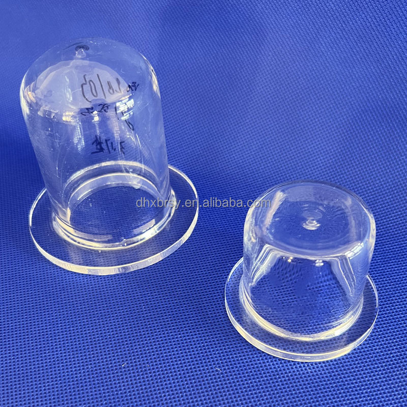
518 Best Quality High Transmittance Fused Quartz 99.99% Silica Content ROHS Certified Clear Photovoltaic Cell Sintering Furnace
View Technical Specs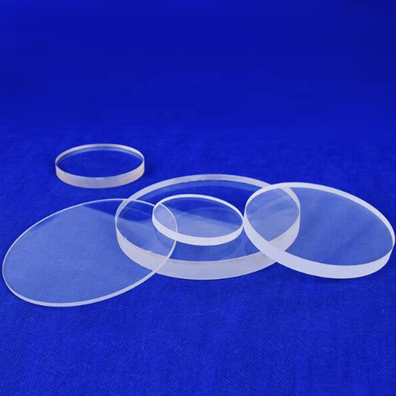
High-purity Polishing Fused Quartz Plate/Sheet Disc 200 Mesh 99.99% Silica Content ROHS Certified BAO RAN Optical Grade Laser
View Technical Specs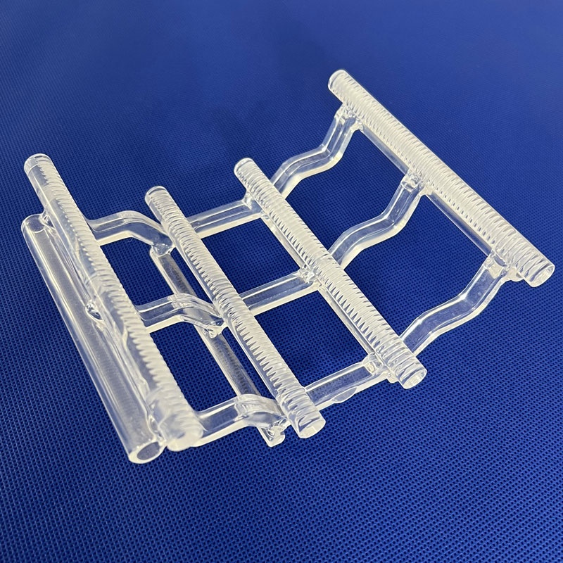
Custom Size High Temperature Fused Quartz Wafer Boat 99.99% Silica Content ROHS Certified Semiconductor Processing Carrier
View Technical Specs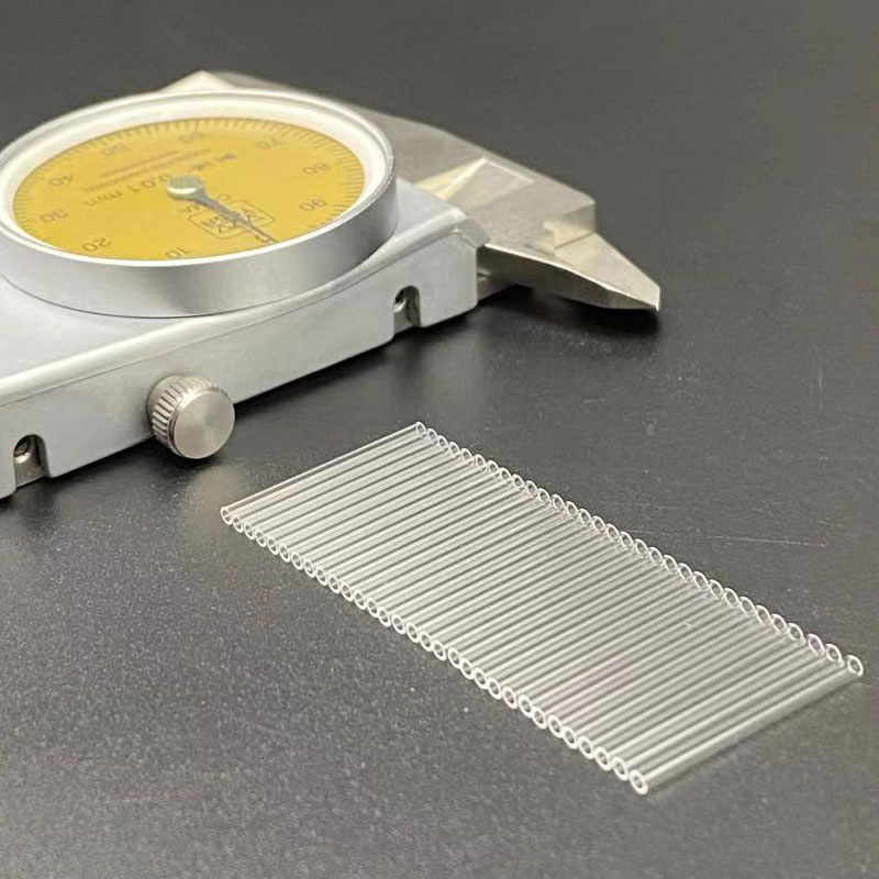
BAO RAN 419 Best Selling 0.1mm 0.2mm 0.3mm 0.4mm 0.5mm Quartz Sheet 99.99% Silica Content SiO2 ROHS Certified 200 Mesh for Laser
View Technical Specs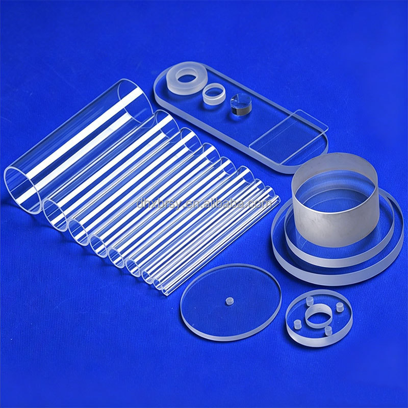
BAO RAN JGS1 High-purity 99.99% SiO2 Temperature Optical Semiconductor Quartz Jig CNC Machined Fused Silica Window UV
View Technical Specs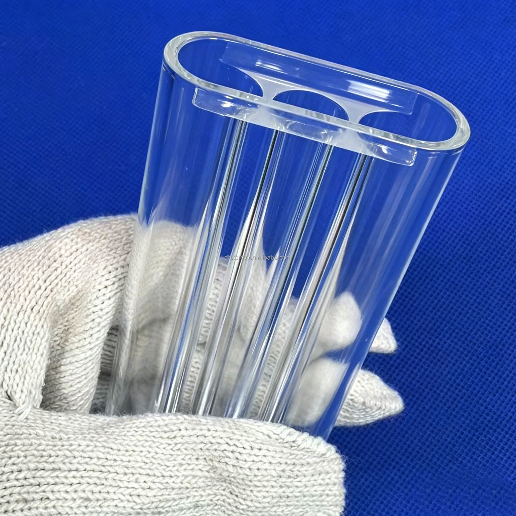
916Factory Customized Quartz Glass Tubes High Temperature Fused Silica Quartz Glass Tube for Lab Furnace Semiconductor Industry
View Technical Specs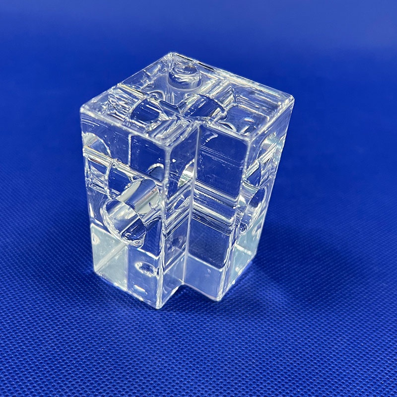
420 BAO RAN Custom-processed Fused Quartz High-purity 99.99% SiO2 ROHS Certified 200 Mesh (75m) Annealed 1200C Fluidic
View Technical Specs
Metropolitan Lisbon Focus
High-Tech Integration in Greater Lisbon's Innovation Hubs
Serving critical industrial facilities across Taguspark (Oeiras), Madan Parque (Caparica), and academic cleanrooms at Instituto Superior Técnico with SEMI-compliant quartz components.
Microelectronics & Bio-MEMS Cleanrooms
Research units along the Tagus corridor utilize our double-side polished (DSP) synthetic quartz wafer discs (100mm, 150mm, and 200mm) as biocompatible, dielectric substrates for microfluidic chips, lab-on-a-chip diagnostic cells, and acoustic wave resonators requiring low auto-fluorescence.
Thermal Diffusion & LP-CVD Furnaces
For advanced solar cell research and thin-film passivation lines in Setúbal and Sintra, our high-purity (≥99.99% SiO₂) diffusion furnace tubes and slot-welded quartz boats resist devitrification under prolonged operation up to 1150°C, preventing metallic trace cross-contamination.
Deep-UV & Telecom Photonics
Integrated photonics groups developing photonic integrated circuits (PICs) rely on our JGS1 grade fused silica windows. With superior optical transmission from 185 nm to 2500 nm, these substrates deliver non-distorting wave-front performance for UV photolithography masks and beam combiners.
Industry Trajectory
Evolving Sourcing Demands in Portugal’s Semiconductor Sector
Under the European Chips Act and national digitization initiatives, Portugal's high-tech manufacturing landscape is experiencing rapid modernization, imposing tighter requirements on raw material purity and delivery pipelines.
99.99%
SiO₂ Chemical Purity
<0.5nm
Surface Roughness (Ra)
1100°C
Continuous Thermal Limit
100%
Polarization Stress Tested
Sub-Nanometer Surface Roughness
Nanofabrication institutes are shifting from standard mechanical lap-polishing to advanced Chemical Mechanical Planarization (CMP). Our Lisbon clients demand surface roughness Ra ≤ 0.5 nm with Total Thickness Variation (TTV) below 5 µm to eliminate focal offsets during e-beam lithography.
Thermal Shock & Thermal-Expansion Matching
With Portugal expanding wide-bandgap (SiC and GaN) epitaxy research, thermal performance is non-negotiable. Our pure quartz carriers offer a coefficient of thermal expansion (CTE) of 5.5 × 10⁻⁷ /°C, drastically minimizing wafer warping and mechanical shock during high-temperature thermal cycling.
Localized Supply Chain Resiliency
Portuguese procurement managers face severe European stockouts. Direct collaboration with our SGS onsite-verified manufacturing facilities eliminates tier-2 trading markups, guarantees batch-to-batch traceability, and provides rapid air cargo transit directly into Lisbon Humberto Delgado Airport (LIS).
Material Comparison
Engineered Quartz Substrate Matrix
Benchmark our optical and semiconductor glass classifications before finalizing fabrication drawings and purchase orders.
| Characteristic / Parameter | JGS1 (Synthetic Fused Silica) | JGS2 (Optical Flame-Fused Quartz) | JGS3 (Electrically Fused Quartz) |
|---|---|---|---|
| SiO₂ Purity Level | ≥ 99.999% (Ultra-pure) | ≥ 99.99% | ≥ 99.98% |
| Dominant Optical Range | 185 nm – 2500 nm (Deep-UV) | 220 nm – 2500 nm (Standard Optical) | 260 nm – 3500 nm (Extended IR) |
| Hydroxyl (OH⁻) Concentration | < 1000 ppm (Controlled) | ≈ 150 – 200 ppm | < 10 ppm (Bubble-free) |
| Continuous Working Temp. | 1100 °C | 1100 °C | 1150 °C |
| Primary Cleanroom Application | Photolithography masks, UV optics | Observation windows, sight glasses | IR sensors, thermal viewports |
| Available Polish Grades | 40/20, 20/10 Scratch-Dig, CMP | 60/40, 40/20 Scratch-Dig | Commercial Polish, Fine Ground |
Enterprise Credentials
Why Lisbon Procurement Directors Source Directly from Our Plant
Uncompromising industrial rigor backed by independent third-party audits and direct source integration.
SGS Onsite-Verified Facility
Our 14,271 m² production infrastructure in Lianyungang operates under complete onsite verification by SGS Group. We handle the entire chain in-house: raw quartz crushing, chemical acid pickling, furnace pulling, and automated CNC five-axis milling.
Certified Stress Testing
Devitrification and micro-cracking occur under internal mechanical stress. Every single boat, tube, and custom-lapped wafer is cycled through automated annealing furnaces (up to 1215°C) and individually checked via polarization stress testers prior to shipping.
Engineered ODM Customization
From single-piece laboratory prototypes to multi-thousand production series, our technical sales engineers parse STEP, DWG, and PDF technical drawings, advising on optimal dimensional tolerances (±0.02 mm), edge chamfering, and flat-ground orientations.
Export-Grade Protective Packaging
Fragile, ultra-thin quartz sheets (0.1 mm) and precision wafer boats are packaged in dust-free Class 10,000 cleanroom environments, utilizing custom vacuum blister packing, shock-absorbing high-density polyethylene foams, and reinforced export-grade wooden cases.
Procurement Clarity
Purchasing FAQ for Portuguese Buyers
Key details regarding regulatory compliance, lead times, custom manufacturing, and international logistics.
How do you handle shipping logistics and customs clearing into Lisbon?
We routinely supply engineering teams and industrial facilities throughout Portugal under standard Incoterms (DAP, DDP, CIF, or FOB). Orders shipped via express air freight typically clear customs at Lisbon Humberto Delgado Airport (LIS) within 4 to 7 business days. All shipments include complete commercial invoices, certificates of conformity (CoC), and detailed packing lists to ensure seamless clearance with the Portuguese Tax and Customs Authority (Autoridade Tributária e Aduaneira).
What documentation is provided to satisfy EU RoHS and cleanroom trace-metal audits?
Every delivery can be accompanied by an official RoHS Compliance Certificate, verifying that hazardous substances (lead, cadmium, mercury, hexavalent chromium, PBB, PBDE) remain well below EU legal thresholds. In addition, for semiconductor-grade wafers, we supply detailed ICP-MS (Inductively Coupled Plasma Mass Spectrometry) impurity reports tracking trace elements (Fe, Cu, Ni, Na, K, Li, Al) down to parts-per-billion (ppb) levels.
Can we purchase prototype quantities (1 to 5 pieces) for research validation?
Yes. We support university laboratories, R&D centers, and advanced technology startups across Greater Lisbon with low Minimum Order Quantities (MOQs) starting from 1 to 5 pieces on standard and custom-machined items. This enables full design verification, thermal testing, and lithography trial runs prior to committing to production-scale batches.
What mechanical tolerances can your CNC machines achieve on custom quartz apparatus?
Our five-axis CNC machining, precision surface grinders, and ultrasonic drilling centers routinely achieve linear dimensional tolerances of ±0.05 mm, and down to ±0.02 mm upon request. For optical surfaces and wafer substrates, we provide surface parallelism < 10 arcseconds, flatness down to λ/4 @ 632.8 nm, and scratch-dig specifications reaching 20/10.
How do you prevent breakage of delicate quartz products during international transit?
Our multi-tier export packaging has been tested and refined across thousands of fragile deliveries worldwide. Wafers are packed in semiconductor-grade cassette boxes or individual coin trays. Complex, welded quartz apparatus—such as wafer boats or triple-bore flow tubes—are suspended inside multi-layer polyurethane foam shock blocks and housed within custom-reinforced wooden cases. We maintain a zero-breakage guarantee on properly handled air-cargo shipments.
Accelerate Your Precision Quartz Project in Lisbon
Whether you require standard JGS1 wafers, customized thermal diffusion boats, or complex CNC-milled fused silica glass assemblies, our engineering staff is available to provide technical feasibility analyses and comprehensive quotations.
Get a Quote