Custom Chamber
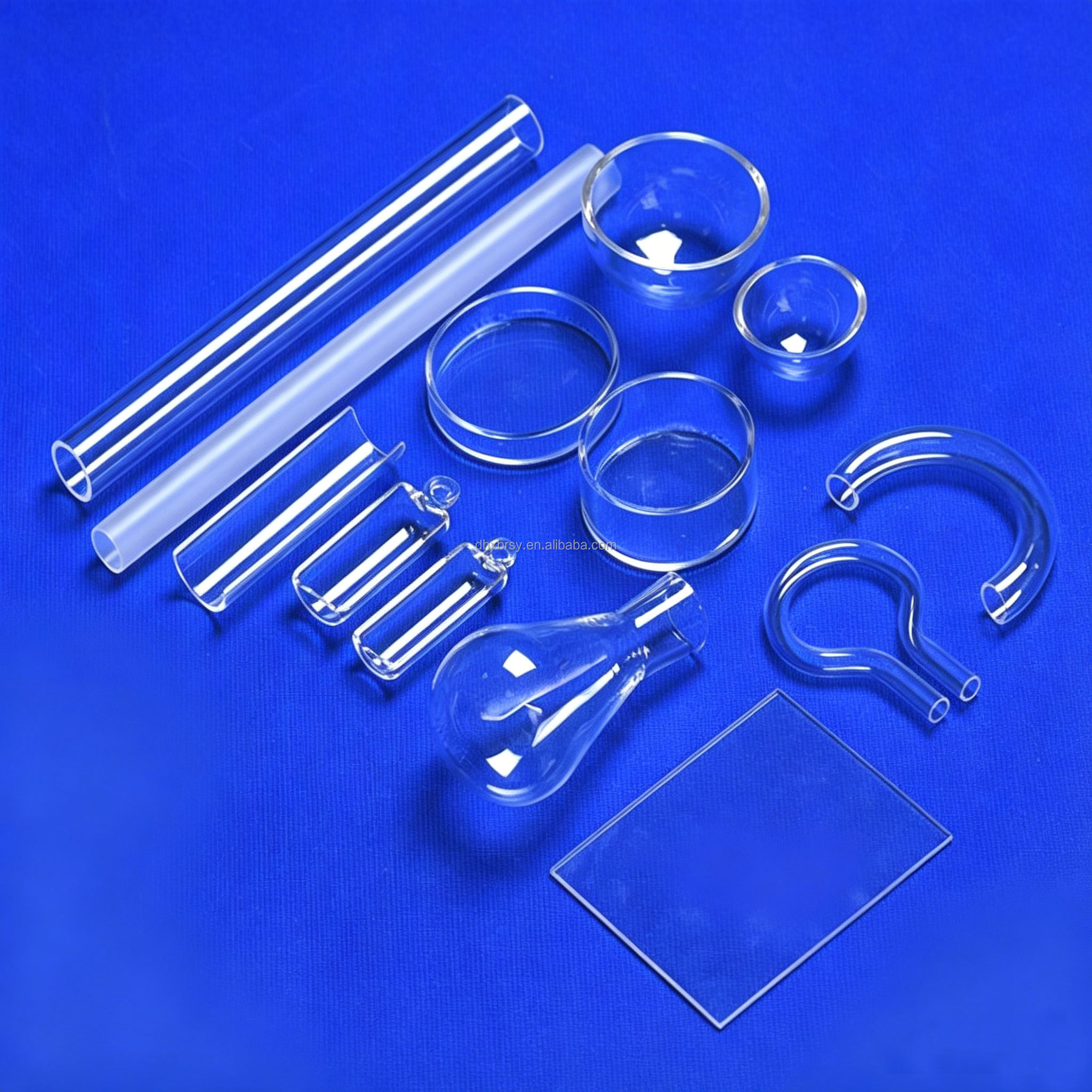
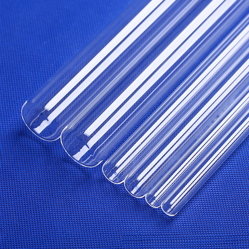
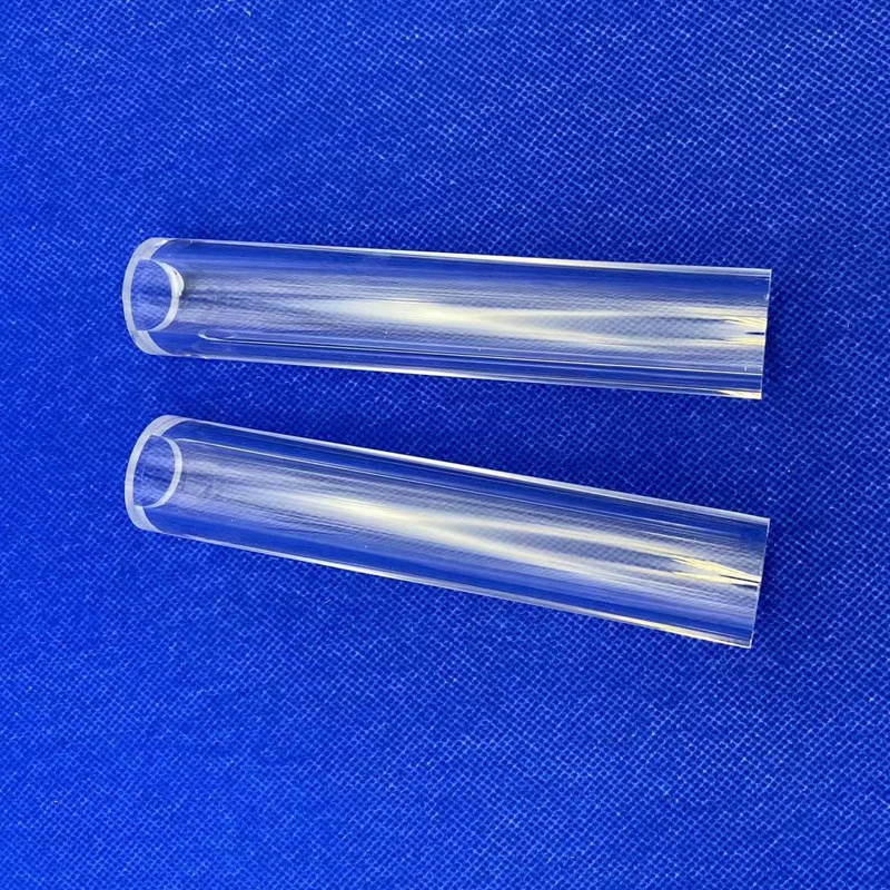
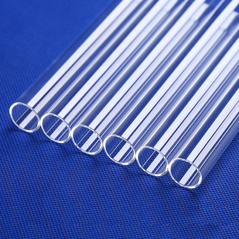
Standard, cleanroom-ready fused quartz plates, multi-bore tubes, and precision machined components designed to withstand critical corrosive environments, deep-UV transmission loss, and extreme thermal shock.
Understanding atomic structural mechanics, trace metal contaminants, and vacuum ultraviolet transmittance characteristics to prevent catastrophic yields losses in sub-5nm lithography and wafer processing.
For instrumentation engineers and procurement directors across San Jose, Santa Clara, Sunnyvale, and Fremont, sourcing the right grade of fused quartz plate is critical. A standard natural quartz plate will solarize, crack, or bubble under excimer UV exposure, while synthetic fused silica provides deep-UV transmission down to 185 nm without darkening.
| Classification | Material Synthesis Base | Spectral Transmission Band | Hydroxyl (OH⁻) Content | Typical San Jose Tech Applications |
|---|---|---|---|---|
| JGS1 (Synthetic Silica) | Synthesized via SiCl₄ oxyhydrogen flame | 185 nm – 2,500 nm (DUV to NIR) | High (≈ 800–1200 ppm) | Photomask substrates, UV laser optics, wafer steppers, laser windows |
| JGS2 (Optical Quartz) | Refined natural quartz crystal melted by oxyhydrogen | 220 nm – 2,500 nm (UV to NIR) | Medium (≈ 150–200 ppm) | Cleanroom sight glasses, spectroscopy cells, UV lamp envelopes |
| JGS3 (Infrared Quartz) | Electrically vacuum-fused natural quartz crystal | 260 nm – 3,500 nm (Full NIR/MWIR) | Ultra-low (< 5 ppm, water-free) | Thermal furnace observation viewports, pyrometry plates, IR sensors |
Fused quartz features an extraordinarily low coefficient of thermal expansion (CTE ≈ 5.5 × 10⁻⁷ /°C), rendering it completely invulnerable to thermal shocks that shatter borosilicate or sapphire glasses. An engineer can heat a 99.99% SiO₂ quartz plate to 1,150°C and plunge it directly into ice water without micro-cracking.
| Physical Property Parameter | Standard Metric Value | Procurement Engineering Significance |
|---|---|---|
| Silicon Dioxide (SiO₂) Purity | ≥ 99.99% (Electronic Grade up to 99.999%) | Prevents metallic ion (Fe, Cu, Na) cross-contamination in fabs. |
| Continuous Service Temperature | 1,100 °C (1,383 K) | Compatible with atmospheric LPCVD, diffusion, and sintering furnaces. |
| Strain / Annealing Point | 1,120 °C / 1,215 °C | Baseline for our internal controlled polarization stress relief furnaces. |
| Dielectric Strength (20°C, 1MHz) | 25–40 kV/mm | Ideal for RF chucks, semiconductor insulators, and high-voltage electrodes. |
How Bay Area advanced manufacturing clusters leverage custom precision quartz glass plates, tubes, and carriers across mission-critical fabrication nodes.
Bay Area fab facilities and equipment refurbishers in North San Jose require high-purity JGS1 fused silica plates for beam splitters, collimation optics, and wafer stage chuck covers. Zero bubble inclusion (DIN ISO 10110 Class 0) ensures uninterrupted laser coherence.
Leading chipmakers and fab suppliers throughout Silicon Valley rely on 99.99% SiO₂ quartz plates as etch chamber liners, viewports, and acid baths. Chemically unreactive to hot HCl, HNO₃, and H₂SO₄, quartz protects wafers from destructive metal ion leaching.
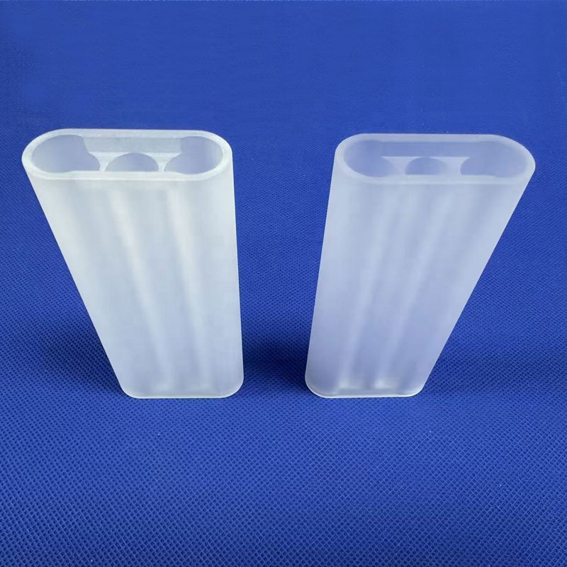
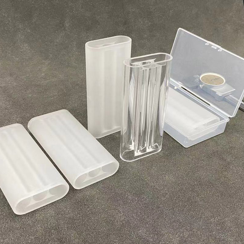
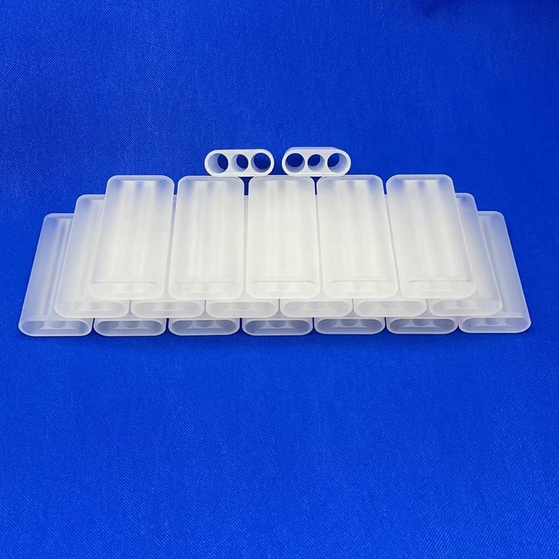
Supplying triple-bore laser cavity flow tubes and multi-hole quartz plates to laser innovators in South Bay and East Bay. Precision dimensional indexing (OD/ID ±0.03mm) accommodates high-repetition Nd:YAG, Alexandrite, and femtosecond medical laser engines.
Clean energy laboratories and clean-tech startups along the I-880 corridor utilize custom fused quartz boats, paddle plates, and sintering furnace tubes capable of withstanding 1,300°C transient thermal runs during NextGen solid-state battery thermal processing.
San Jose life science accelerators rely on precision CNC-drilled fused quartz 96-well microplates and optical flow cells for deep-UV fluorescence analysis, genome sequencing, and extreme temperature sterilization where standard polymers fail.
Particle accelerator experiments, quantum computing incubators, and thin-film PVD chambers employ our custom CF/ISO flanged quartz viewports tested down to 10⁻¹⁰ Torr ultra-high vacuum with helium leak mass spectrometry inspection.
Shifts in semiconductor packaging, CHIPS Act incentives, and lead-time mitigation are fundamentally transforming how California tech giants source raw silica components.
Historically, Bay Area research institutions and fab lines relied on regional glass distributors who imposed markups of 300% to 500% with opaque 12-to-16-week delivery horizons. Today, San Jose supply chain directors bypass local middlemen, purchasing directly from primary ISO/SGS-audited factories that control the mineral chain from natural quartz pulverizing to final laser CNC cutting.
As semiconductor manufacturing in the Silicon Valley ecosystem transitions toward heterogeneous chiplet integration and glass carrier substrates, allowable trace impurities are plummeting. Sodium (Na), Potassium (K), and Iron (Fe) levels must remain below 0.1 ppm to avoid mobile ion contamination during temporary wafer bonding and thermal release processes.
An objective evaluation framework based on SGS on-site audits, raw material independence, precision CNC fabrication capacity, and export compliance to California ports.
| Rank & Manufacturer | Core Specialization | Material Purity & Range | Lead Time to San Jose (SJC/OAK) | Sourcing Suitability Index |
|---|---|---|---|---|
| 01. Lovri Quartz Products Co., Ltd. | Full-cycle custom fused quartz plates, CNC machining, triple-bore tubes & wafer boats | 99.99% SiO₂; JGS1, JGS2, JGS3, Opaque | Express: 5–7 days; Air: 10–12 days | Tier 1: Best for Custom Drawing Prototyping & Fab Direct |
| 02. Heraeus Conamic | Large diameter synthetic silica ingots & semiconductor plasma chambers | High purity Suprasil® / Spectrosil® | 8–14 weeks (Standard distribution) | Tier 1: Global conglomerate for bulk raw ingots |
| 03. Tosoh Quartz, Inc. | Fabricated quartzware for semiconductor wafer processing equipment | Semiconductor-grade clear silica | 6–10 weeks | Tier 1: High-volume OEM equipment supplier |
| 04. Momentive Technologies | Fused quartz tubing, crucible production, and matrix rods | High purity natural quartz | 8–12 weeks | Tier 2: Primary raw material ingot producer |
| 05. QSil SE (formerly Schott Quartz) | Plasma torches, quartz cylinders, and high-temp furnace tubes | Pure fused silica & doped quartz | 6–12 weeks | Tier 2: High-temperature European industrial components |
| 06. Technical Glass Products (TGP) | Specialty optical glass windows, custom lab apparatus, and plates | Commercial quartz & Pyrex stock | 2–4 weeks (US Stock distribution) | Tier 2: Local US stocking warehouse distributor |
| 07. CoorsTek Silicon Valley Ops | Engineered ceramics and precision machined quartz sub-assemblies | Engineered ceramics & quartzware | 4–8 weeks | Tier 2: Specialty custom ceramic-quartz assemblies |
| 08. Lianyungang Pacific Quartz (Pacific New Materials) | Mass production of quartz sand, standard photovoltaic tubing | Natural solar grade quartz | 3–6 weeks | Tier 3: Bulk solar cell production raw materials |
| 09. Shin-Etsu Quartz Products Co. | Synthetic quartz substrates for photomasks and semiconductor rings | Synthetic electronic silica | 10–16 weeks | Tier 3: High-end Japanese semiconductor photomasks |
| 10. Swift Glass Company | Custom glass fabrication, thermal tempering, waterjet glass cutting | Commercial optical glasses | 3–5 weeks | Tier 3: Broad industrial glass cutting & processing |
By operating our own raw mineral crushing, chemical acid pickling, automatic tube drawing, and 5-axis CNC machining, we eliminate outsourcing defects and deliver verified performance.
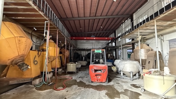
Located in Lianyungang, China's quartz capital, we pulverize, rescreen, and acid-pickle silica sand directly in-house. Achieving 99.99% SiO₂ purity at the mineral stage ensures structural homogeneity and zero metallic ion outgassing.
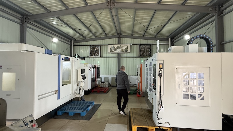
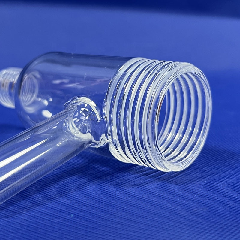
Equipped with ultra-high-speed diamond tooling, ultrasonic drilling, and computerized edge slotting. We execute micro-channel quartz plates, threaded reaction tubes, stepped sight windows, and 96-well plates to exact CAD/STEP geometries.
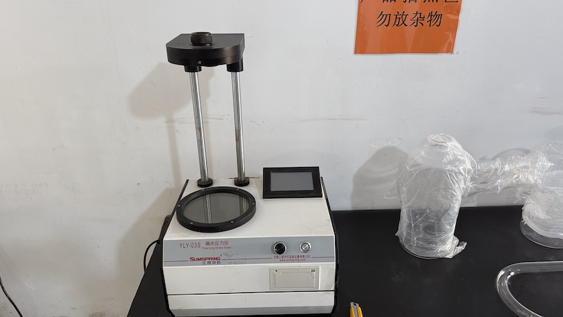
Residual internal stress is the single greatest hidden cause of explosion in thermal furnaces. Every batch is heat-treated in digital annealing furnaces up to 1,215°C and validated using optical polariscopes before leaving the factory.
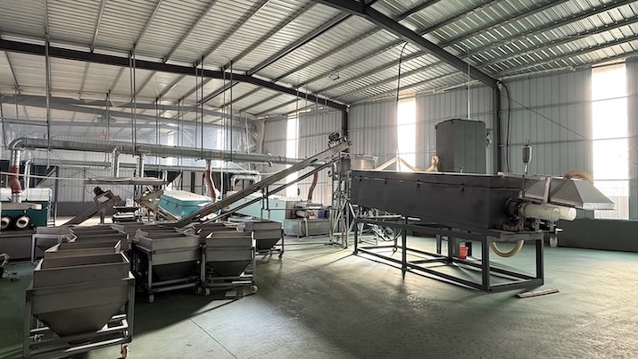
Shipped safely across the Pacific to San Jose (SJC), San Francisco (SFO), and Oakland (OAK). Components are packed with dust-free static-neutral wraps, high-density impact foams, and moisture-sealed reinforced timber crates.
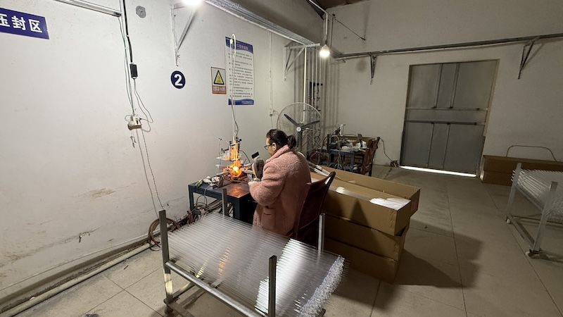
Combining lathe-guided automation with master scientific glassblowers. We seamlessly fuse quartz flanges, multi-port branch elbows, and one-end closed flat or domed bases capable of sustaining ultra-high vacuum environments.
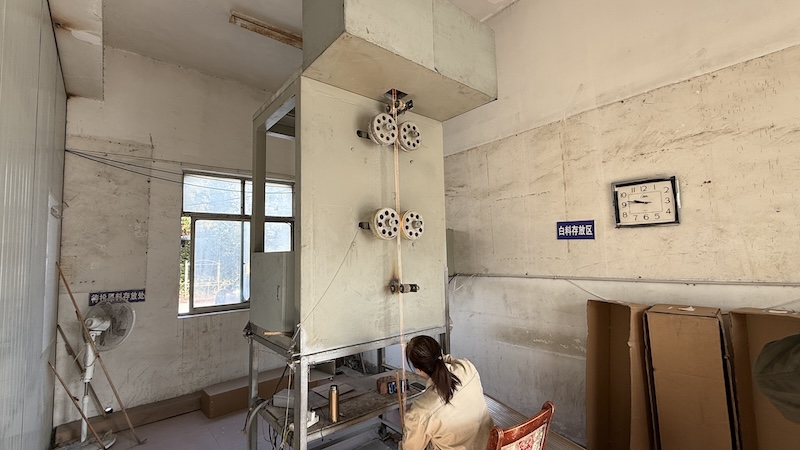
Our 14,271 m² manufacturing campus has undergone full on-site assessment by SGS Group. We supply full trace metallurgy documentation, RoHS restricted substance reports, and dimensional inspection sheets with every shipment.
Clear, expert answers to the most common questions raised by Silicon Valley equipment designers and corporate purchasing departments.
Quartz plates and tubes imported into California typically enter under HTS Code 7002.31.00 (fused quartz tubes) or 7006.00.00 / 7017.10.00 (laboratory and industrial quartzware). We routinely support DDP (Delivered Duty Paid) shipping via air express (FedEx/DHL/UPS) or air freight to San Jose International (SJC) or SFO, where all clearance, tariffs, and local freight are managed smoothly with transparent door-to-door pricing.
Because we maintain in-house JGS1, JGS2, and JGS3 raw quartz sheets and rods, prototype manufacturing typically takes 3 to 7 working days from drawing sign-off. Combined with priority air express, custom CNC machined parts frequently arrive at your Santa Clara or San Jose cleanroom within 10 to 14 calendar days.
Yes. Our engineering department operates with 3D CAD platforms accepting .STEP, .IGES, .DWG, and .DXF file formats as well as annotated PDFs. We perform immediate manufacturability reviews (DFM), verifying draft angles, minimum wall thicknesses, and chamfer transitions to optimize strength and prevent thermal cracking.
We employ a specialized 5-layer export packaging protocol: individual dust-free vacuum wrapping, anti-static bubbles, surrounding shock-absorbing high-density polyethylene (EPE) closed-cell foam, intermediate crash cartons, and custom-built shock-isolated plywood crates. Our transit damage rate to US buyers remains under 0.1% over verified export cycles.
We supply quartz plates with commercial cut/fine-ground edges, flame-polished finishes, or double-sided precision optical polishing. For laser optics and semiconductor inspection windows, we achieve surface roughness down to Ra < 0.5 nm (80/50 or 60/40 scratch/dig standards, with 40/20 or 20/10 available on demand), and optical flatness within 1 to 2 lambda per inch.
We maintain a low-friction entry threshold: prototype orders have an MOQ of just 1 to 5 pieces for custom plates, tubes, or CNC components. This allows Silicon Valley hardware teams and university labs (Stanford, UC Berkeley, SJSU) to validate designs before scaling to volume production.
Send your DWG, STEP, or PDF drawing today. Receive a comprehensive DFM manufacturability evaluation, raw material purity report, and transparent direct-factory quote within 24 hours.