Semiconductor Pipeline
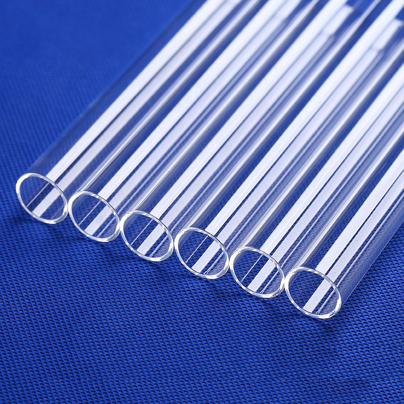
Clear Quartz Tubing OD 10/14/20mm Heat Resistant
Semiconductor wet etching cleaning pipeline and flame-worked welding bending with high structural purity and thermal shock endurance.
Direct from factory production lines: 99.99% SiO₂ precision manufactured plates, CVD chambers, CNC sub-assemblies, and deep-UV optical transmission materials built to ultra-tight mechanical tolerances.
Semiconductor wet etching cleaning pipeline and flame-worked welding bending with high structural purity and thermal shock endurance.
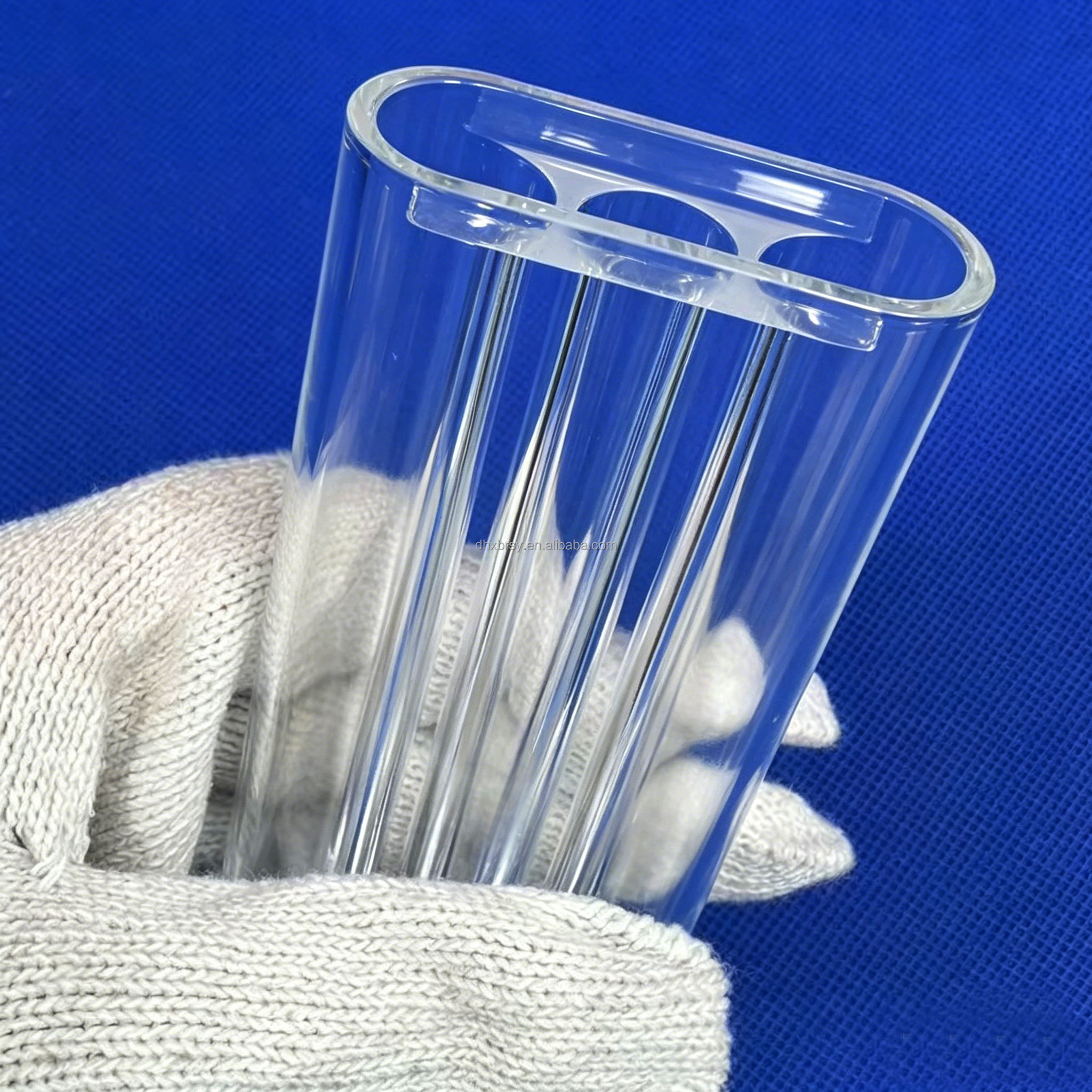
Designed for heavy industrial thermal processing, high-vacuum lab furnaces, and precision semiconductor diffusion lines.
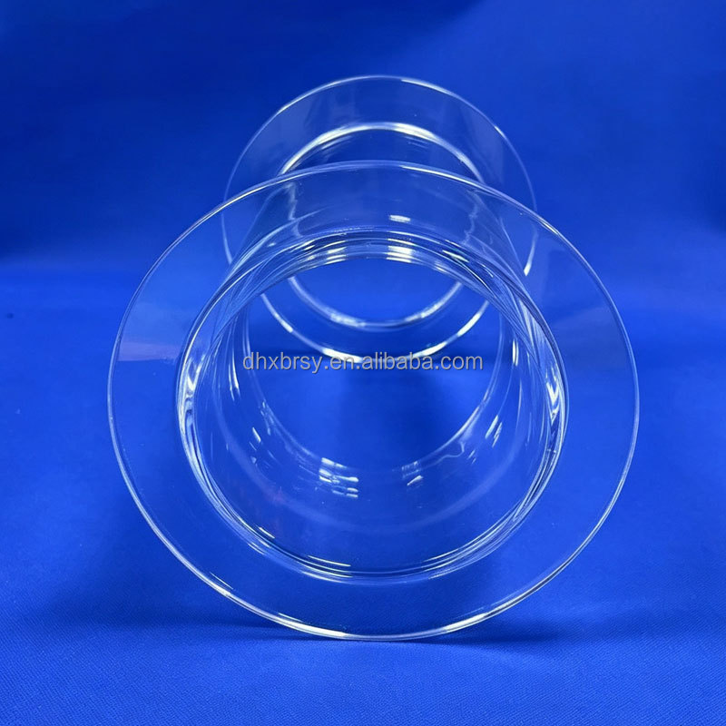
Seamless transparent fused silica cylinder with dual precision-ground vacuum flanges engineered for chemical vapor deposition (CVD).
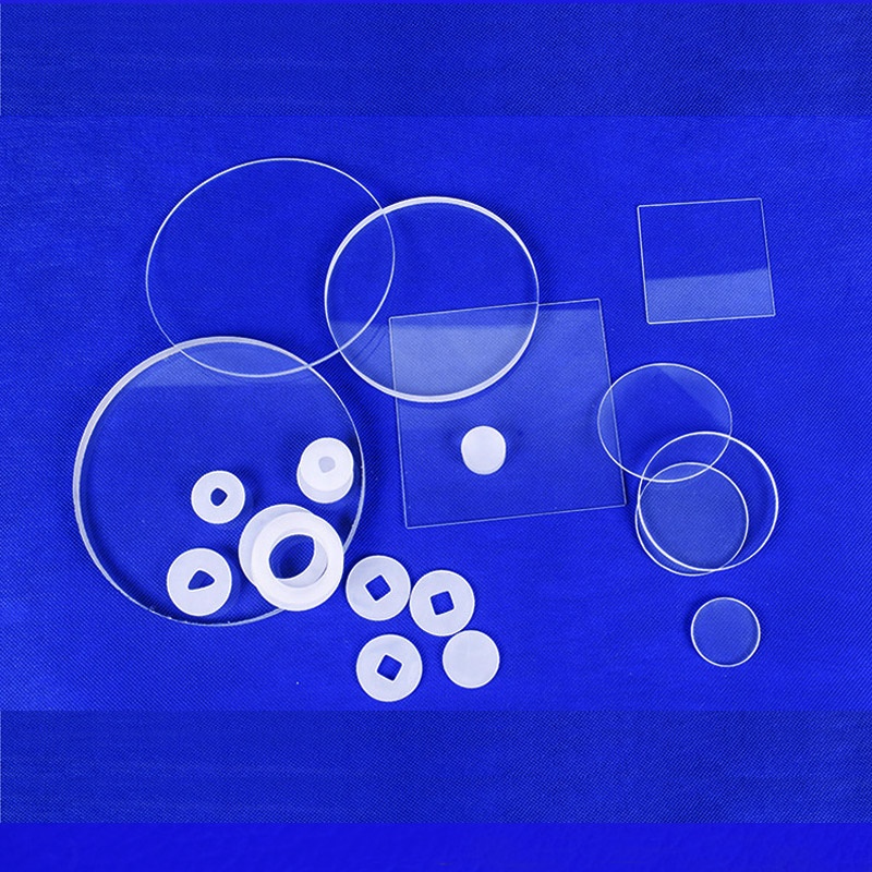
Deep ultraviolet transparent synthetic silica plate annealed for excimer lasers, optical lithography, and high-frequency optoelectronics.
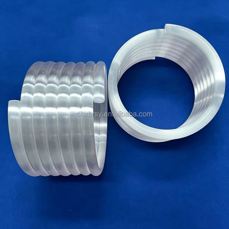
Micro-bubble diffuse reflection geometry optimized for high-efficiency infrared thermal emitters and chemical continuous heaters.
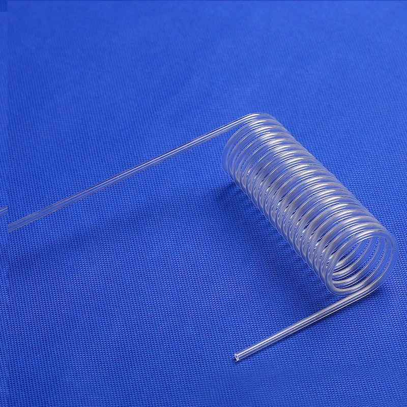
Specialized optical filtering spiral sleeve designed for aesthetic laser pumping cavities and medical high-intensity pulsed lamps.
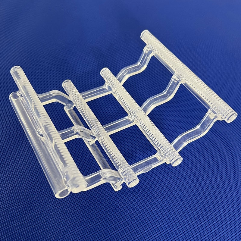
Ultra-pure slot-pitch carrier manufactured to nanometer-grade surface smoothness, resistant to continuous 1100°C furnace ramp cycles.
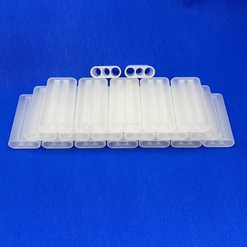
Complex multi-channel precision fused assembly delivering matched cooling fluid velocities and high pump efficiency for industrial laser heads.
Synthetic fused silica and naturally fused quartz plates represent the cornerstone of next-generation optical, lithographic, and wafer-handling infrastructures. Unlike ordinary borosilicate or soda-lime glass substrates, fused silica plates (amorphous silicon dioxide, SiO₂) deliver near-zero thermal expansion coefficients (approx. 5.5 × 10⁻⁷ /°C), broad optical transmission extending from deep ultraviolet (185 nm) through the mid-infrared spectrum (3,500 nm), and exceptional dielectric isolation under high thermal bias. As semiconductor nodes advance below 3nm, and high-power industrial fiber lasers surge past 20 kW thresholds, component failure resulting from trace metal contamination, devitrification, or sub-surface micro-cracks is completely unacceptable.
This benchmark report examines the Top 10 Fused Silica Plate Factories and Suppliers globally, providing mechanical engineers, cleanroom facility procurement managers, and optical physicists with quantifiable criteria to navigate optical homogeneity grades, OH⁻ content variations, synthetic chemical vapor deposition (CVD) methods, and electric fusion processing capabilities.
The global production of fused silica substrate plates is heavily stratified. Top-tier manufacturers are separated by raw material control, thermal annealing kinetics, optical stress birefringence levels, and CNC finishing precision. Below is the procurement-level comparison of the premier global entities supplying semiconductor-grade and high-spec optical silica plates.
| Manufacturer / Supplier | Primary Headquarters | Core Material Competency | Standard Purity (SiO₂) | Typical Applications |
|---|---|---|---|---|
| Lovri Quartz Products Co., Ltd. | Lianyungang, China | Full in-house supply: Pulverizing to CNC polishing & JGS1 plates | 99.99% – 99.999% | Semiconductor CVD, UV laser windows, wafer boats, lab apparatus |
| Heraeus Conamic | Kleinostheim, Germany | Suprasil® synthetic silica, low OH⁻ fused quartz ingots | 99.9999% | EUV lithography optics, microlens arrays, telecom boules |
| Corning Incorporated | New York, USA | HPFS® 7980, extreme ultraviolet (EUV) optical glass blanks | 99.9999% | Space exploration mirrors, stepper optics, excimer systems |
| Tosoh Quartz Corporation | Tokyo, Japan | Semiconductor-grade large quartz masking plates & CVD flanges | 99.995% | Diffusion furnace internal hardware, plasma etch rings |
| Shin-Etsu Chemical | Tokyo, Japan | Synthetic quartz substrates, photomask blanks | 99.9999% | Photolithography mask substrates, optical wafer carriers |
| Saint-Gobain Quartz | Courbevoie, France | Quartzel® fibers, high-temperature thermal barrier plates | 99.99% | Aerospace thermal blankets, radomes, high-spec furnaces |
| Momentive Technologies | Ohio, USA | Electrically melted quartz (Puranal®), high-viscosity plates | 99.995% | Solar silicon crucible linings, heavy wafer thermal processing |
| Edmund Optics | New Jersey, USA | Precision coated optical windows, JGS1/Corning polished flats | 99.99% – 99.999% | Metrology viewports, beam splitters, laboratory photonics |
| Nikon Glass Solutions | Tokyo, Japan | Ultra-homogeneous synthetic silica blocks and plates | 99.9999% | Laser processing objectives, high-NA illumination components |
| CoorsTek | Colorado, USA | Structural engineered ceramics, hybrid fused silica fixtures | 99.99% | Wafer handling end-effectors, aggressive plasma hardware |
When engineering and sourcing a fused silica plate, specifying "quartz glass" without designating the material synthesis route frequently results in catastrophic application mismatch. In international trade and precision metrology, silica plates are predominantly categorized across three primary transmission classifications:
1. JGS1 (Synthetic Fused Silica / Deep-UV Grade): Synthesized from volatile silicon compounds (such as SiCl₄) oxidized inside a high-temperature oxyhydrogen flame. This manufacturing protocol eliminates metallic impurities (Fe, Al, Ti < 0.1 ppm). JGS1 demonstrates remarkable transmission spanning from 185 nm to 2,500 nm, containing essentially zero bubble inclusions. It is impervious to laser-induced darkening (solarization) and is mandatory for 193nm/248nm excimer laser systems, medical aesthetics, and high-energy ultraviolet disinfection viewports.
2. JGS2 (Flame-Fused Quartz / Optical Grade): Produced by gas refining premium-grade natural quartz crystals. It offers consistent optical clarity across the ultraviolet-to-visible spectra (220 nm to 2,500 nm). JGS2 contains negligible structural micro-striations and provides the primary balance between cost-efficiency and optical performance for industrial sight glasses, analytical spectrometer windows, and high-intensity discharge lamp housings.
3. JGS3 (Electrically Fused Silica / Infrared Grade): Melted under protected vacuum or neutral electric heating elements. Because this process suppresses hydroxyl bonding, JGS3 possesses an exceptionally low OH⁻ concentration (typically < 5 ppm). Consequently, it completely eliminates the intense absorption band at the 2,730 nm wavelength, enabling smooth, uninterrupted transmission from 260 nm upwards to 3,500 nm. JGS3 is widely specified for pyrometric viewports, infrared heating systems, and aerospace thermal sensors.
The global demand profile for fused silica plates is undergoing structural reorganization fueled by three massive macro-technological transitions:
Trend 1: Accelerated Wafer Scaling and 3D Heterogeneous Packaging
As advanced packaging paradigms (CoWoS, chiplet integration) proliferate, the thermal stability requirements for wafer-level processing carriers have become stringent. Traditional mechanical boats are rapidly transitioning toward precision-machined fused silica carriers with coefficient of thermal expansion (CTE) matching that of silicon wafers down to ±0.05 × 10⁻⁶/K across 20°C–800°C ranges, reducing warpage risks.
Trend 2: Vertically Integrated Mineral Refining to Suppress Trace Aluminum
Global supply chain volatility has made reliance on third-party purified raw sand a critical risk. Sourcing entities are actively qualifying manufacturers that control chemical refining, pulverizing, and acid washing internally. By eradicating trace alkali and aluminum ions early, manufacturers avoid surface devitrification (cristobalite crystal seeding) when furnace tubes and plates operate at sustained temperatures above 1150°C.
Trend 3: Nanometer-Level Sub-Surface Damage (SSD) Mitigation in CNC Polishing
Standard mechanical lapping inevitably leaves microscopic fissures beneath the optical surface. Future procurement specs demand magnetorheological finishing (MRF) or precision chemical-mechanical polishing (CMP) yielding scratch-dig ratings of 10-5 or 20-10, with surface roughness (Ra) maintained strictly below 0.3 nm, ensuring zero laser scatter and minimal chemical etching erosion under CF₄/CHF₃ plasma chemistries.
Situated in the heart of China’s premier silica processing hub (Tuofeng Industrial Park, Lianyungang, Jiangsu), Lovri Quartz Products Co., Ltd. offers an integrated manufacturing model that eliminates international procurement middlemen while maintaining strict global verification credentials.
Spanning 14,271 m² of advanced workshop space, our facilities and full chemical processes have completed on-site auditing by SGS Group. RoHS and CE compliance are systematically documented across all custom production lots.
We control the complete pipeline from raw quartz chunk crushing and mechanical pulverizing to multi-stage acid pickling. This internal capability guarantees consistent 99.99% SiO₂ content and shields buyers from upstream raw supply shocks.
Every customized batch is annealed in computer-controlled electric ovens and tested on digital polarization stress meters to eliminate internal tension. Our 5-axis CNC machines deliver complex laser-welded and slotted geometries directly from STEP/DWG files.
Direct answers addressing technical parameters, dimensional tolerances, packing integrity, and export logistics.
Ready to initiate technical consultation or receive a competitive factory-direct quote?
Contact Us