Engineered Quartz Glass & Optical Substrate Showcase
Verified manufacturing specifications covering double-sided polished plates, semiconductor reaction vessels, precision V-grooves, and furnace components conforming to international RoHS and CE certifications.
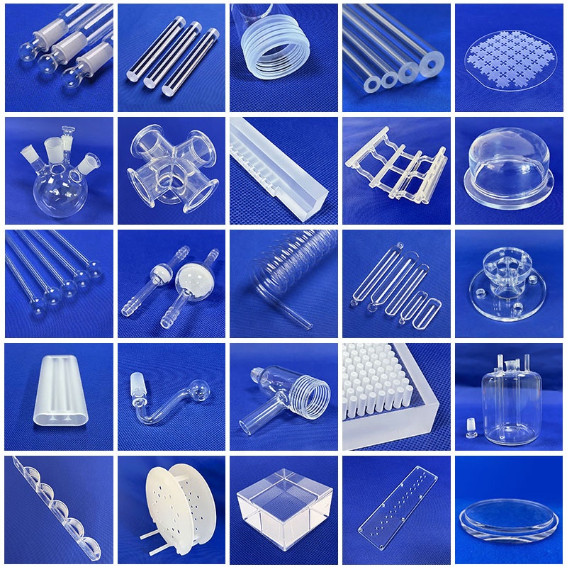
BAO RAN 419 Corrosion Resistant High Light Transmittance Double Sided Polishing White Rim Fused Quartz Sheet
99.99% SiO₂ content, optical grade double-sided chemical-mechanical polishing (CMP), ultra-low bubble inclusion class, high deep-UV transmittance.
View Specifications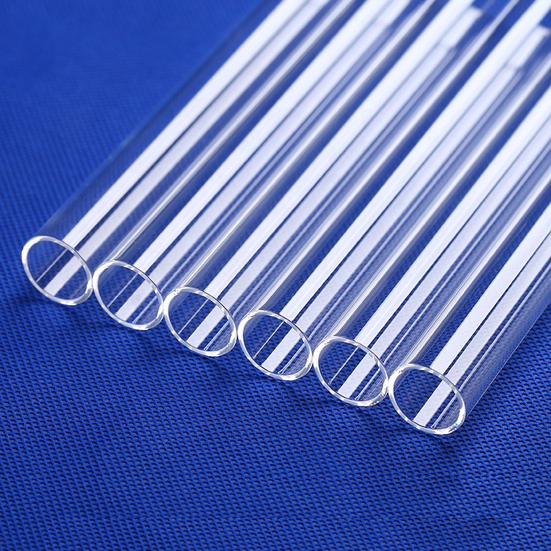
High Precision Clear Quartz Glass Tubing OD 10mm/14mm/20mm Heat Resistant Cleaning Pipeline
Tight dimensional wall tolerances (±0.05 mm), continuous service at 1100 °C, optimized for hot acid cleaning lines, bending, and flame welding.
View Specifications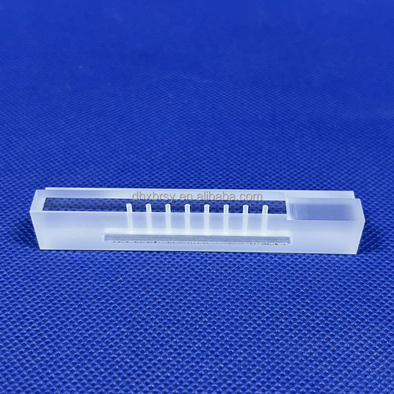
High Purity Fused Quartz V Groove Fixture Precision Machined Fiber Array Holder
Micron-level CNC slotting, zero thermal expansion hysteresis, ideal for DWDM laser collimators and optical communication alignment platforms.
View Specifications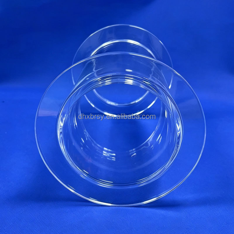
Custom High Purity 99.99% Transparent Fused Silica Quartz Cylinder Double Flange
Precision ground sealing faces, high-vacuum helium leak rate tested, zero micro-cracking at flanges for LPCVD/PECVD epitaxial deposition chambers.
View Specifications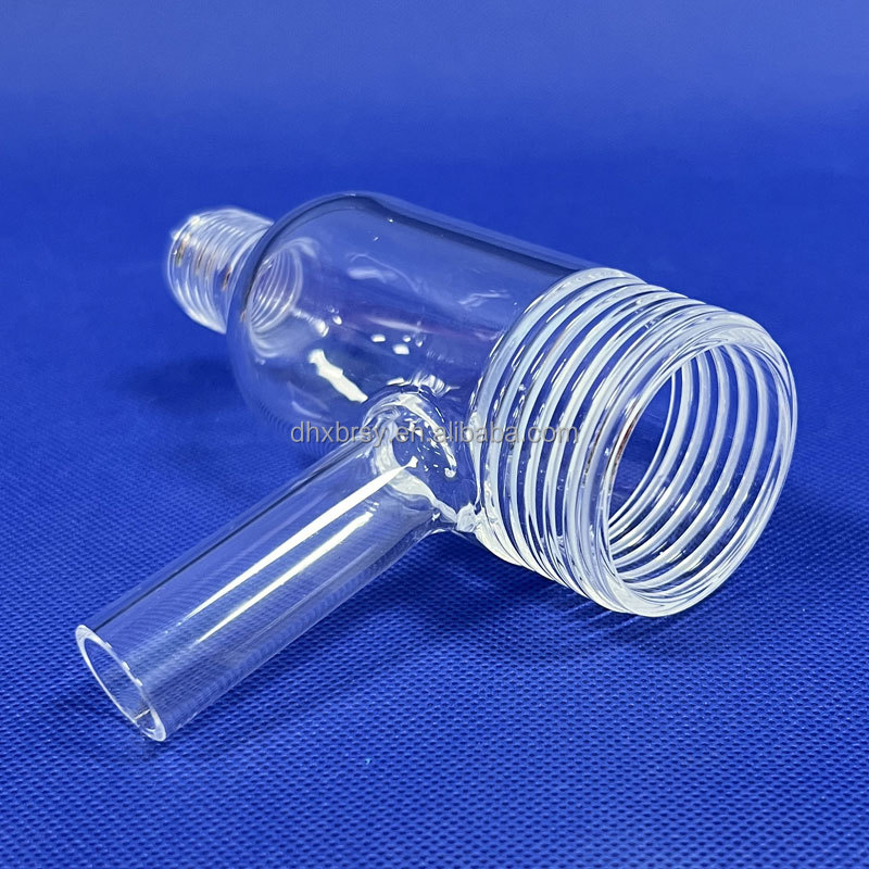
High Quality Polished Tube High-Temperature Threaded Quartz Glass Tube ROHS
Custom standard and metric screw profiles, seamless fire-polished surface finish, high corrosion immunity against harsh halogens and plasma etch.
View Specifications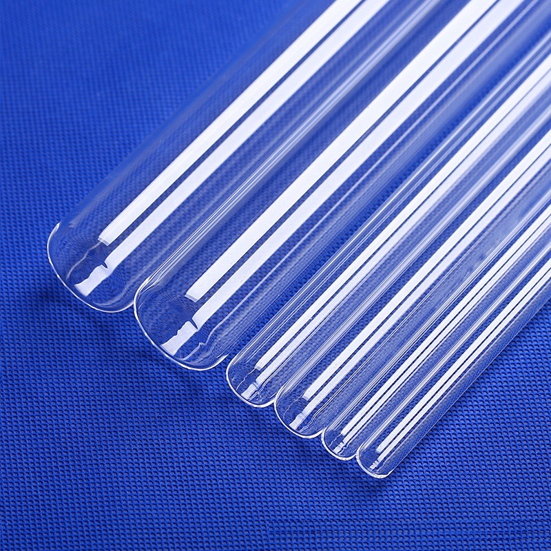
Customized Clear Quartz Glass Tube Fused Silica One End Closed Bottom
Uniform bottom wall thickness distribution, round or flat domed bottom, thermal shock resistance to sudden 1100 °C quench into water.
View Specifications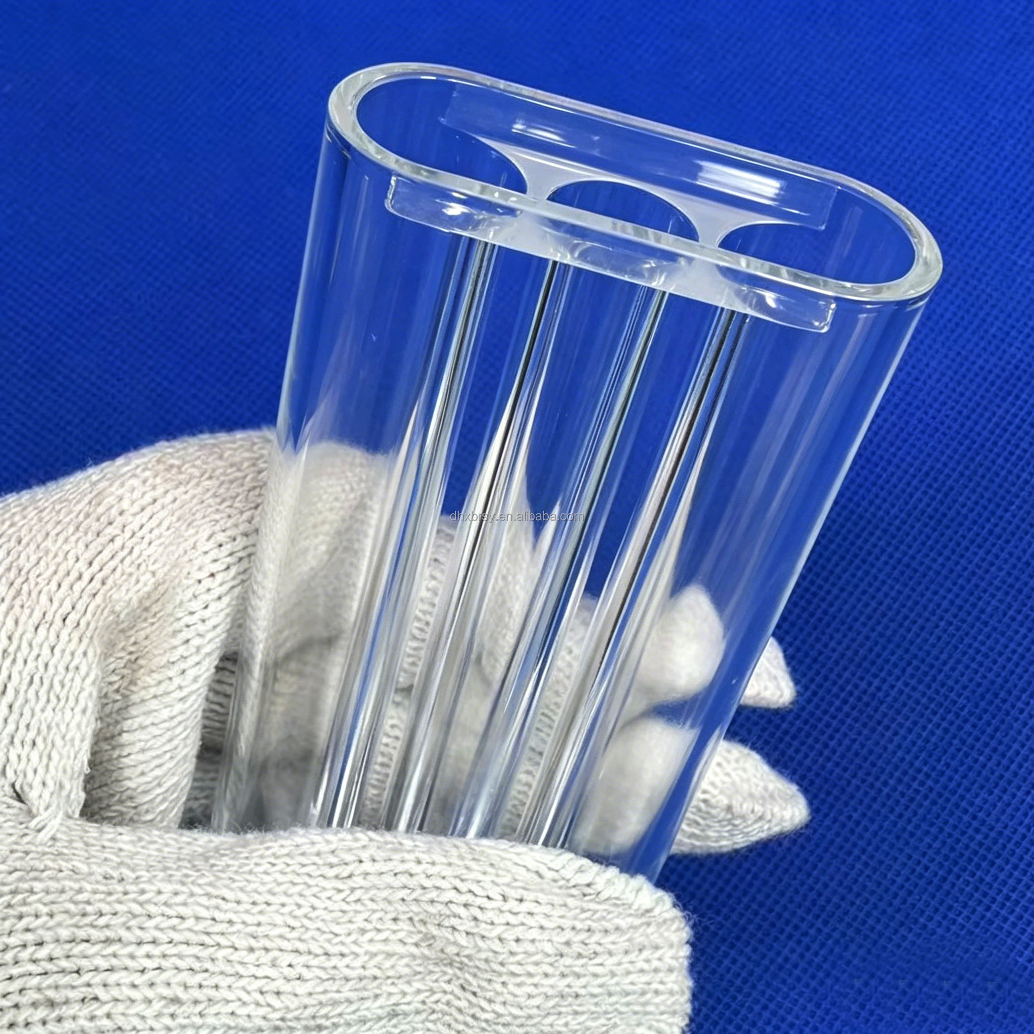
916Factory Customized Fused Silica Quartz Glass Tube for Lab Furnaces
Engineered for large-bore thermal tube furnaces, heavy devitrification resistance under alkaline atmospheres, low hydroxyl content profile.
View Specifications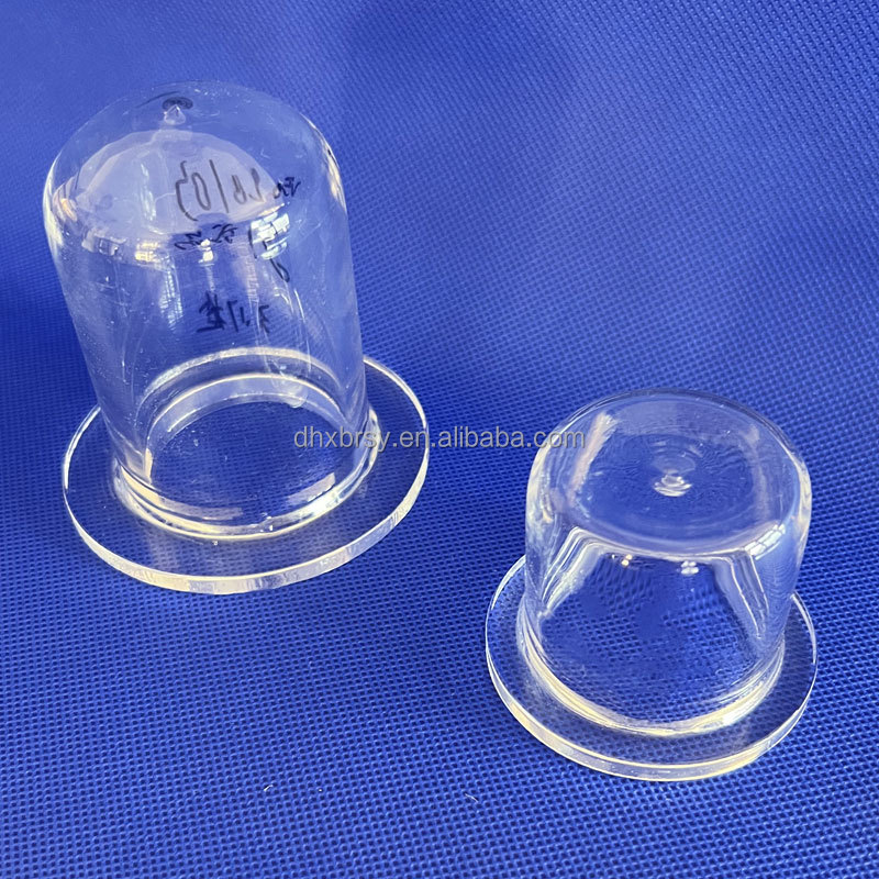
518 High Transmittance Fused Quartz for Photovoltaic Cell Sintering Furnace
Optimized spectral transmission across infrared and visible bandwidths, superior structural rigidity avoiding sag during high-temp continuous solar runs.
View SpecificationsIndustrial Landscape: Why China Dominates the Global Fused Quartz Plate Supply Chain
In modern advanced optics, wafer fabrication, and high-intensity ultraviolet curing, the fused quartz plate serves as an irreplaceable baseline material. Composed of non-crystalline silicon dioxide (SiO₂) in an amorphous molecular matrix, precision quartz plates offer unmatched thermal stability, dielectric isolation, and broadband spectral transmittance ranging from the deep vacuum ultraviolet (VUV) spectrum through the near-infrared (NIR) wavelengths. Over 75% of global high-purity natural silica reserves and downstream fused quartz manufacturing capacity are concentrated within China—specifically centered in the Tuofeng Industrial Park in Lianyungang, Jiangsu Province.
Global procurement executives, semiconductor equipment integrators, and optical laboratory researchers choose Chinese fused quartz manufacturers not solely for cost competitiveness, but for the extensive vertical integration found in clusters like Lianyungang. The local supply chain incorporates every process stage within a narrow 15-kilometer radius: from raw lump selection and chemical acid washing to thermal continuous drawing, high-temperature electric arc fusing, internal polarization stress relief, and multi-axis CNC grinding. This industrial density eliminates middleman logistics, compresses lead times for custom bespoke components from weeks to days, and ensures rigid consistency across massive production batches.
Selecting a certified manufacturer like Lovri Quartz Products Co., Ltd. (verified onsite by the SGS Group across a 14,271 m² production facility) provides procurement engineers with technical accountability. Unlike simple cutting workshops that outsource blanks of questionable origins, fully integrated Chinese factories control the chemical leaching of raw quartz sands to eliminate trace transition metals (iron, copper, titanium) down to parts-per-billion (ppb) thresholds, securing long-term devitrification resistance under continuous operational cycles up to 1100 °C.
Technical Material Selection Matrix: JGS1 vs. JGS2 vs. JGS3 Quartz Grades
A frequent cause of catastrophic optical breakdown or unexpected budget escalation is the misapplication of quartz glass grades. Chinese optical standards classify fused silica plates into three definitive grades based on raw material provenance, synthesis method, and hydroxyl radical [OH⁻] concentrations. Understanding these parameters is crucial for matching the correct grade to the operating environment:
| Optical Grade | Synthesis Process | Spectral Window | Hydroxyl [OH⁻] PPM | Primary Industrial Applications |
|---|---|---|---|---|
| JGS1 (UV Grade) | Synthetic SiCl₄ vapor phase deposition | 185 nm – 2,500 nm | < 20 – 100 ppm | Deep-UV excimer lasers, lithography stepper windows, high-resolution spectroscopy cuvettes, UV-C germicidal windows. |
| JGS2 (Optical Grade) | Oxyhydrogen flame fused natural quartz | 220 nm – 2,500 nm | 150 – 200 ppm | Semiconductor furnace observation sight glasses, UV curing lamps, solar cell sintering carriers, chemical observation viewports. |
| JGS3 (IR Grade) | Electric vacuum furnace melted silica | 260 nm – 3,500 nm | < 5 ppm (Water-free) | High-temperature infrared heaters, CO₂ laser output couplers, military thermal imaging covers, pyrometer protective sight glasses. |
| Opaque Quartz | Gas-bubble enriched fusion method | Diffuse scattering / IR block | Variable | Thermal radiation baffles, semiconductor CVD flange insulation rings, heat shields for rapid thermal processing (RTP). |
Lovri Quartz: In-House Production & Metrology Standards
Touring the engineering infrastructure that enables tight dimensional control and strict optical verification from raw crystal to finished component.
Source Sand Acid Leaching
We do not rely on pre-ground commercial quartz sand of unknown origin. Our plant operates continuous multi-stage hydrochloric and hydrofluoric acid pickling baths that cleanse natural crystal lumps to guarantee ≥99.99% SiO₂ purity, preventing bubble crystallization and premature devitrification under high furnace loads.
5-Axis CNC Precision Machining
Equipped with high-speed diamond tooling centers capable of micro-drilling, complex beveling, slotting, stepped counterbores, and micro-grooving down to ±0.005 mm tolerances. We fabricate complex custom shapes directly from CAD drawings (STEP, DWG, DXF) without tooling die delays.
Polarization Stress Testing
Thermal processing introduces residual internal stress that cannot be detected by the naked eye. In accordance with strict semiconductor QA guidelines, 100% of annealed quartz plates and apparatus are passed through cross-polarization photoelastic analyzers to verify stress birefringence values below 5 nm/cm.
Future Sourcing & Procurement Trends for Fused Quartz Plates
Essential market intelligence for global supply chain leaders navigating the next generation of semiconductor packaging, renewable energy, and optical lithography demands.
CMP & Carrier Plates for Fan-Out Wafer-Level Packaging (FOWLP)
As advanced microelectronics shift toward chiplet architectures and 2.5D/3D packaging, requirements for ultra-flat quartz carrier plates have increased significantly. Wafer bonding platforms now require quartz discs with total thickness variation (TTV) under 1.5 µm and surface roughness Ra under 0.2 nm to prevent bonding voids during mechanical thinning processes.
Suppression of Excimer Laser Radiation-Induced Compaction
Next-generation 193 nm immersion and deep-UV laser systems generate high fluence energy that causes standard quartz to experience density compaction and solarization over time. Future procurement contracts increasingly specify synthetic fused silica with strict hydrogen-loaded passivation to sustain long-term laser damage thresholds (LDT) exceeding 10 J/cm².
Zero-Carbon Electric Arc Smelting & Waste Acid Neutralization
Global environmental mandates (including EU CSRD and carbon border adjustments) are compelling tier-1 silicon fabs to scrutinize upstream quartz smelters. Chinese manufacturers are transitioning from conventional coal-gas oxyhydrogen burners to closed-loop automated electric arc furnaces powered by renewable energy, combined with zero-effluent fluoride recovery systems.
Frequently Asked Questions: B2B Fused Quartz Sourcing
Direct answers from our senior materials engineers covering technical feasibility, production tolerances, international export packaging, and commercial terms.
Accelerate Your Fused Quartz Procurement with Direct Factory Engineering
Whether you require standard JGS1 optical blanks, tight-tolerance CNC micro-machined fixtures, or large-format semiconductor reaction cylinders, our Lianyungang engineering team will review your technical drawings and provide a competitive quote within 24 hours.
Get a Quote