SiO₂ 99.99%
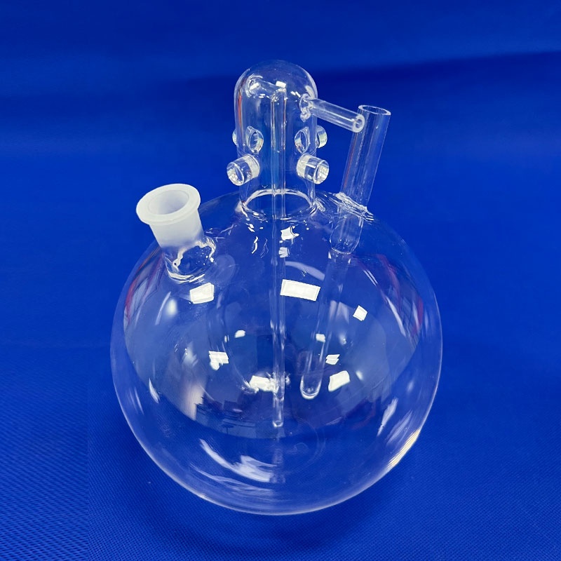
Direct from the factory: standard and tailored fused silica apparatus, double-side polished wafer plates, laser reactors, and thermal tubes engineered to tight geometric tolerances (±0.02 mm) and tested for near-zero residual stress.
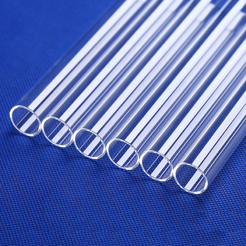
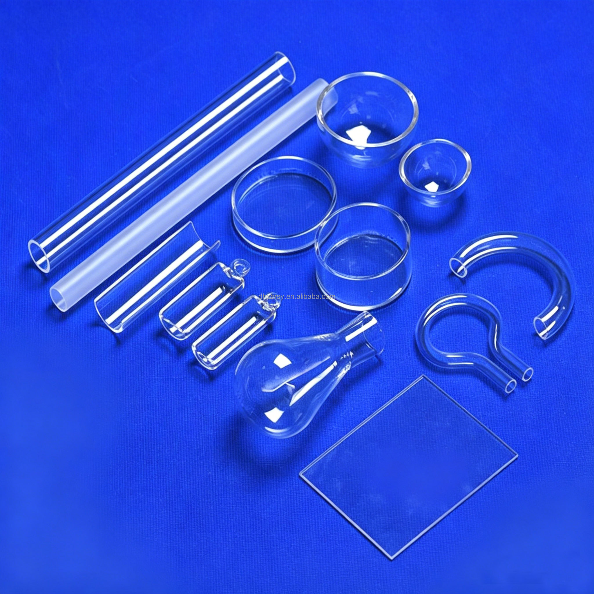
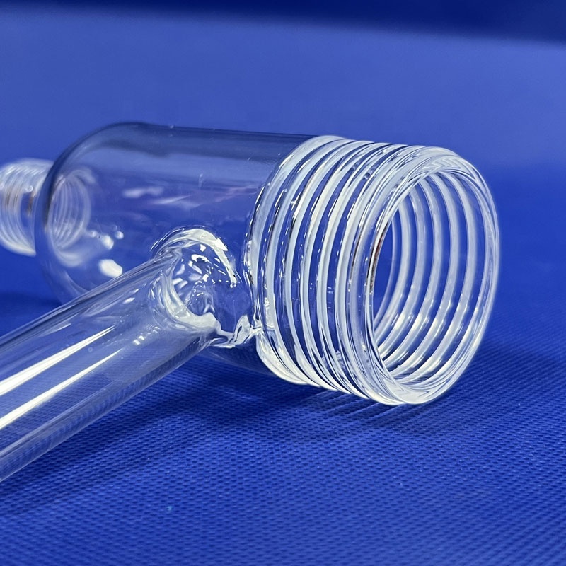
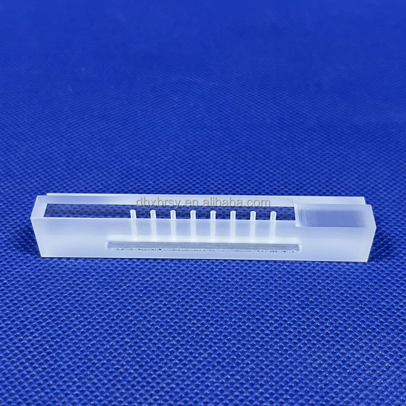

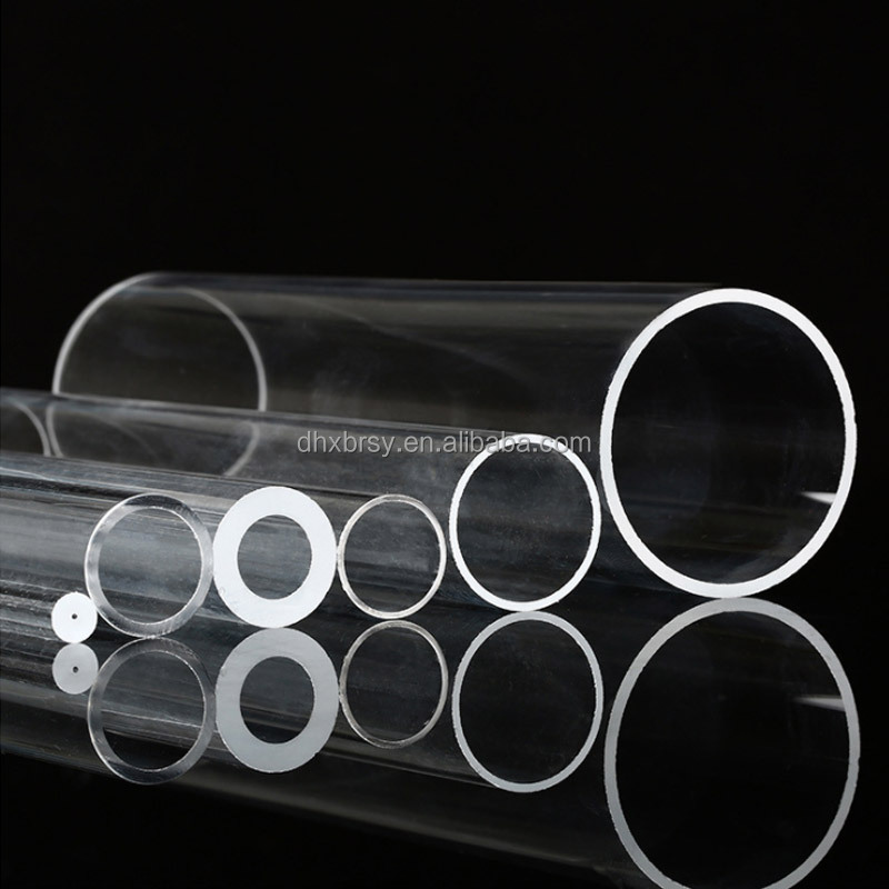
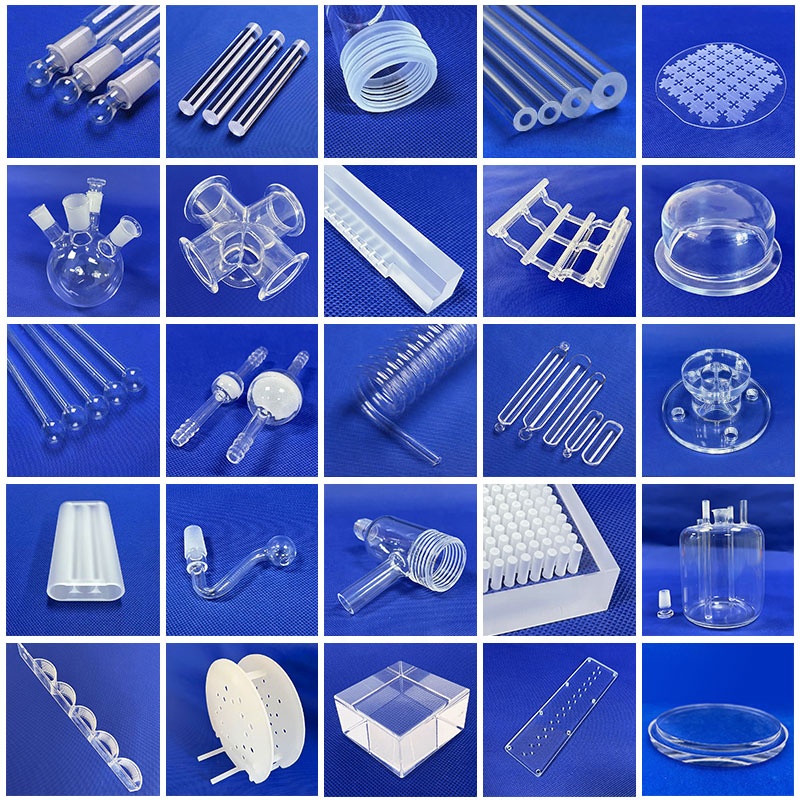
A comprehensive examination of synthetic fused silica versus natural fused quartz substrate performance in high-temperature, vacuum, and deep-ultraviolet lithography environments.
In modern industrial fabrication, quartz glass substrates (fused silica / SiO₂) represent the indispensable backbone for photolithography mask blanks, optoelectronic packaging, thin-film wafer carriers, and high-frequency microwave windows. Unlike standard borosilicate or soda-lime glass, fused quartz is composed purely of silicon dioxide in an amorphous, non-crystalline state. This monolithic chemical structure imparts exceptional thermal stability, near-zero thermal expansion coefficient (approx. 5.5 × 10⁻⁷ /°C), extreme optical transmission across the deep-ultraviolet (DUV) to near-infrared (NIR) spectrum (185 nm to 3,500 nm), and unsurpassed dielectric strength.
Critical Engineering Principle: For applications in extreme cleanroom environments and chemical vapor deposition (CVD), quartz substrates eliminate the risks of alkali ion diffusion (Na⁺, K⁺, Ca²⁺) that plague conventional glasses. With trace metal impurity profiles controlled down to parts-per-billion (ppb) tiers through multiple hydrochloric and hydrofluoric acid-pickling cycles, our fused quartz substrates guarantee complete process inertness at operating regimes exceeding 1,100 °C.
Depending on the designated working waveband and thermodynamic loads, substrate selection in Southeastern European industrial projects predominantly centers on four specialized classifications:
1. JGS1 (Synthetic Fused Silica): Synthesized via high-temperature chemical vapor oxidation of silicon tetrachloride (SiCl₄). Free of visible micro-bubbles and metallic impurities, JGS1 exhibits outstanding transmission in the deep UV band (>90% at 193 nm and 248 nm), making it the prime candidate for excimer laser output windows, UV stepper exposure stages, and high-end spectroscopy flow cells.
2. JGS2 (Optical Grade Fused Quartz): Smelted from premium natural crystalline quartz sand under high-temperature oxyhydrogen flames. Characterized by negligible bubble formation and uniform refractive indices, JGS2 provides superior mechanical strength and UV-visible transparency across 220 nm to 2,500 nm, widely deployed in optical sight glasses, wafer carrier boats, and plasma etching viewports.
3. JGS3 (Infrared Grade Fused Quartz): Electrically fused in high-vacuum resistance furnaces to strip away hydroxyl radicals (OH⁻ content controlled below 2–5 ppm). JGS3 eliminates the severe 2.73 μm infrared absorption band, delivering broad spectral transmission stretching into the mid-infrared region up to 3,500 nm.
4. Opaque & Porous Fused Silica: Sintered with microscopic gaseous cavities to optimize infrared reflectance and thermal insulation, specifically applied in heating diffusers, thermal shields, and epitaxial growth flanges.
| Physical / Chemical Property | Test Standard / Conditions | JGS1 (Synthetic Silica) | JGS2 (Natural Fused Quartz) | Borosilicate 3.3 (Baseline) |
|---|---|---|---|---|
| SiO₂ Purity Tier | ICP-MS Quantitative Analysis | ≥ 99.999% | ≥ 99.99% | ≈ 81% (Alkali doped) |
| Softening Point | Dilatometer / ASTM C338 | 1,730 °C | 1,680 °C | 825 °C |
| Continuous Thermal Threshold | Atmospheric Furnace (Air) | 1,150 °C | 1,100 °C | 450 °C |
| Thermal Expansion (CTE) | 20 °C to 320 °C (10⁻⁷ / °C) | 5.4 | 5.5 | 33.0 |
| Thermal Shock Resistance | Rapid Quenching ΔT (Cold Water) | ΔT > 1,100 °C (No fracture) | ΔT > 1,000 °C (No fracture) | ΔT ≈ 150 °C |
| Surface Roughness (Ra) | Double-Side Chemical Mechanical Polishing | < 0.5 nm (0.2 nm feasible) | < 0.5 nm | ≈ 1.5 – 3.0 nm |
| Dielectric Constant (ε) | 1 MHz at 25 °C | 3.75 | 3.80 | 4.60 |
Bridging global fused silica manufacturing excellence with Bulgaria’s rapidly transforming industrial landscape, from Sofia’s laser physics laboratories to Plovdiv’s mechatronics parks.
Sofia Tech Park and the Bulgarian Academy of Sciences (Institute of Solid State Physics, Institute of Electronics) require JGS1 UV grade fused silica laser reactors, cavity mirrors, and high-damage-threshold beam splitter plates for high-energy femtosecond and diode-pumped solid-state laser experiments.
Within the Thrace Economic Zone (Plovdiv), Tier-1 automotive electronics and sensor manufacturers deploy double-side polished fused quartz wafer blanks as thermal submounts, insulating RF spacers, and optical encoder plates that must endure severe thermal cycles without mechanical deformation.
Botevgrad’s microelectronics legacy is revitalized through specialized semiconductor assembly facilities requiring high-purity quartz wafer boats, vertical furnace diffusion tubes, and acid-resistant etching vessels for wafer-level packaging and discrete semiconductor processing lines.
Renewable solar manufacturing and thin-film pilot plants in Southern and Northern Bulgaria deploy high-transmittance quartz process tubes, heater shields, and anti-reflective coated quartz sheets for cell sintering ovens and solar simulator calibration assemblies.
Municipal water treatment facilities, food packaging lines, and industrial effluent sanitization systems across the Varna and Black Sea logistics corridor implement ozone generator quartz discharge tubes, high-ozone quartz sleeves, and UV-C germicidal reactor vessels.
With Bulgaria ranking among Europe’s top-tier fiber optic and telecommunication infrastructure hubs, CNC precision-machined quartz V-groove arrays and collimator holders serve as critical alignment carriers for single-mode and multicore fiber arrays.
Analyzing the intersection between the European Chips Act, regional nearshoring of advanced mechatronics, and specialized deep-tech microfabrication initiatives.
Bulgaria’s strategic drive to participate in the European Chips Act value chain is fostering localized assembly, test, and packaging (ATP) nodes. Local engineering teams require stable, reliable suppliers of certified quartz substrates with traceable RoHS/CE conformity and rapid prototyping lead times.
Bulgarian instrument makers and optical labs are shifting toward higher surface flatness (λ/10 to λ/20 at 632.8 nm) and extreme parallelism (< 3 arcseconds). Standard float glass is progressively being phased out in favor of high-purity JGS1/JGS2 synthetic fused quartz.
Startups and academic research spin-offs across Sofia and Gabrovo rely heavily on rapid iteration. The standard market demand has moved from rigid catalog ordering to drawing-based custom manufacturing (1 to 5 pieces) without prohibitive tooling or setup charges.
Operating an SGS-verified 14,271 m² production facility in Lianyungang, China—the epicenter of the world’s high-purity silica deposits—we control every manufacturing milestone from raw mineral refining to five-axis CNC machining.
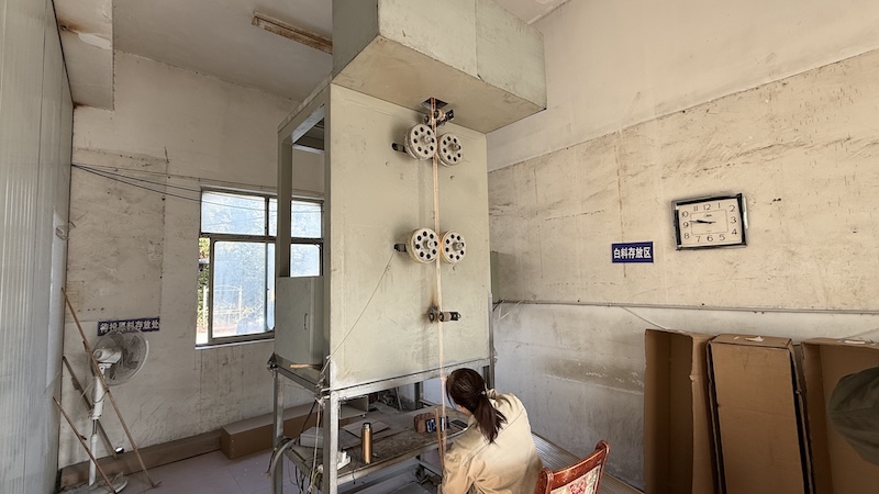
By bypassing third-party trading intermediaries, European buyers gain direct source-level access to 99.99% SiO₂ fused silica raw materials, complete batch traceability, and rapid CAD-to-prototype validation.
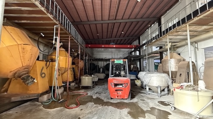
Hot multi-acid pickling strips off metallic iron and alkali oxides to reach certified 99.99% SiO₂ minimum purity.
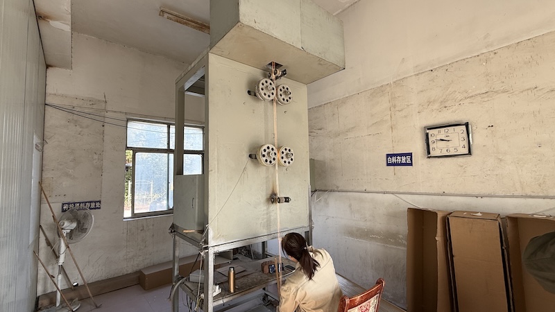
High-temperature furnace drawing into target profiles, followed by diamond wire slicing of substrate wafer blanks.
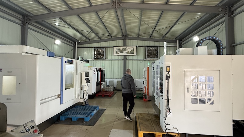
High-speed CNC centers perform contour milling, edge bevelling, slotting, and double-side chemical mechanical polishing.
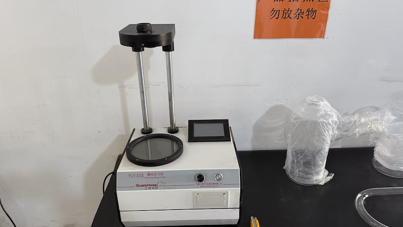
Every piece undergoes polarization stress testing and coordinate measuring machine (CMM) dimensional verification.
Key technical, regulatory, and supply chain insights to assist Bulgarian hardware engineers and procurement managers in specifying fused quartz substrates.
Whether you require standard JGS1 optical windows, high-precision semiconductor wafer carriers, or custom five-axis CNC machined fused silica reactors for your facility in Sofia, Plovdiv, or across the European Union, our technical sales engineers will deliver a comprehensive manufacturability review and competitive factory quote within 24 hours.