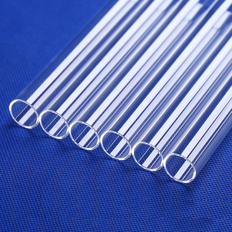
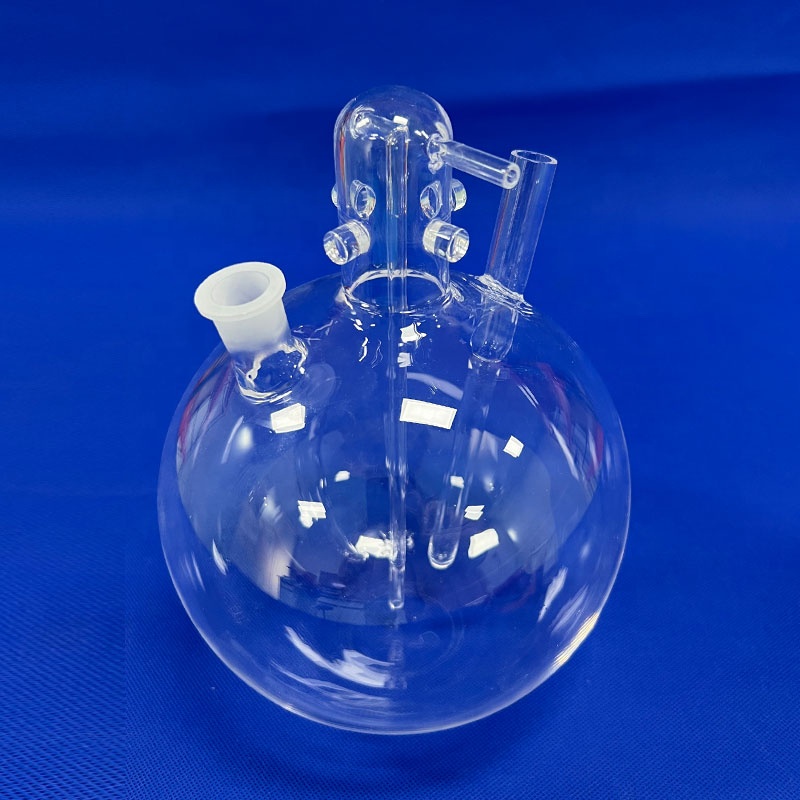
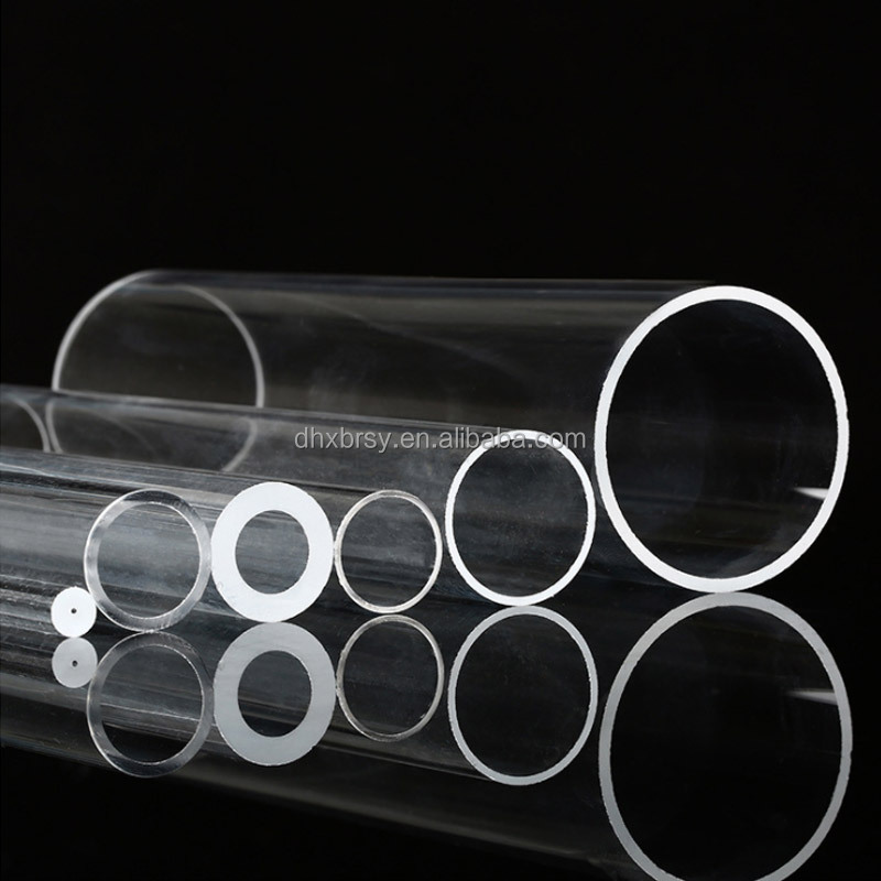
Manufactured under strict class-10,000 cleanroom environments to satisfy demanding thermal, dielectric, and optical specifications across semiconductor, laser machinery, and analytical physics applications.
Situated in China's premier mineral and silica engineering cluster—Lianyungang—Lovri Quartz leverages complete ownership over the manufacturing lifecycle. From direct quartz sand purification and acid leach treating to five-axis CNC milling, diamond cutting, and thermal laser flame-polishing, we eliminate third-party supply vulnerabilities.
14,271 m² Modern PlantDedicated cleanrooms & furnaces
Precision quartz manufacturing demands unwavering chemical stabilization and mechanical discipline at every phase.
1. Hydrodynamic Sand Pickling
Raw granular silica is refined through sequential hot fluorinated and hydrochloric leach processes, purging transition metals (Fe, Ti, Cu) to <0.5 ppm.
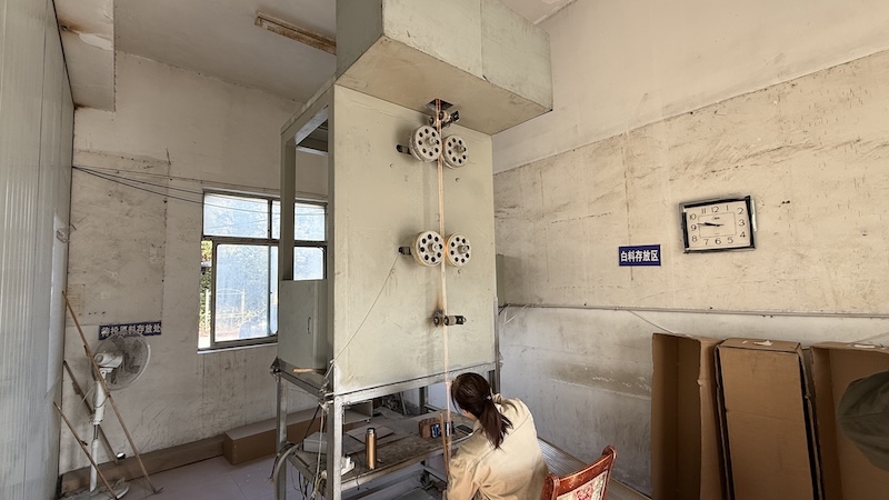
2. Electric Thermal Fusion
Continuous thermal drawing in vacuum resistance crucibles at 2,050°C transforms refined SiO₂ into stress-uniform blocks, ingots, and master cylinders.
3. Diamond Milling & CMP
Substrates are sliced via diamond wire saws, CNC milled with sub-millimeter indexing, and polished via Chemical-Mechanical Planarization (CMP) to Ra <0.5 nm.
4. Polariscopic Metrology
Every substrate batch completes double-pass polariscopic strain birefringence verification, UV-Vis-NIR spectrophotometer mapping, and dimensional laser profiling.
Industry Whitepaper Report
The Strategic Evolution of Custom Quartz Substrates in Advanced Microelectronics
As modern semiconductor manufacturing approaches atomic-scale line widths (sub-3nm lithography nodes) and high-power optoelectronics transition toward extreme ultraviolet (EUV) regimes, the physical requirements placed on optical and structural carrier substrates have surged. Quartz substrates—both synthetically grown (JGS1) and high-purity natural fused silica (JGS2/JGS3)—represent the baseline material of modern wafer transport, optical lithography photomasks, RF MEMS, and photonics interconnect fixtures.
Unlike borosilicate, soda-lime, or aluminosilicate formulations, high-purity fused silica exhibits a near-zero coefficient of thermal expansion (α ≈ 5.5 × 10⁻⁷ /°C between 20°C and 300°C). This structural stability eliminates mechanical warp, pattern displacement, and substrate fatigue during severe thermal transients. In plasma-enhanced chemical vapor deposition (PECVD) and reactive ion etching (RIE) setups, standard commercial glasses disintegrate under harsh fluorine and chlorine radicals; high-density 99.99% SiO₂ substrates resist reactive plasma deterioration, preserving chamber integrity and dramatically curtailing wafer-level particulate contamination.
Key Engineering Fact: Synthetic fused silica substrates synthesized via chemical flame hydrolysis (SiCl₄ + 2H₂ + O₂ → SiO₂ + 4HCl) contain zero bubble defects (DIN ISO 10110 Class 0) and undetectable trace metallic contaminations, driving laser-induced damage thresholds (LIDT) past 15 J/cm² at 355nm (10ns pulses).
Future Procurement Trends in the Global Quartz Glass Ecosystem
Supply chain leaders across North America, Europe, and the Asia-Pacific region are navigating tectonic shifts in advanced material procurement. Three predominant dynamics now dictate how tier-1 semiconductor foundries, analytical equipment builders, and laser systems integrators qualify their quartz substrate exporters:
1. Direct Regional Cluster Sourcing & Disintermediation: For decades, buyers relied on Western distributors that marked up semi-finished blanks originating from primary processing zones. Forward-looking procurement directors now bypass these middlemen, forming direct joint development programs with ISO-certified factory clusters in China (such as Lianyungang). This shift yields 30% to 50% cost reductions while shaving weeks off design iterations for specialized CNC configurations.
2. Tightening Metrological Documentation Requirements: Modern RFQs no longer accept broad material claims. Foundries demand full batch traceability: certificate of analysis (COA) containing ICP-MS elemental breakdown, UV-VIS spectrophotometer transmission charts spanning 190 nm to 3,000 nm, and interferometric surface roughness maps proving sub-angstrom (Ra ≤ 0.5 nm) chemical-mechanical polish finishes.
3. Resilience Against Geopolitical Chokepoints: Given recent trade turbulence, Tier-1 equipment manufacturers are executing dual-vendor strategies, deliberately qualifying agile, independent Chinese export specialists possessing their own acid pickling and synthesis plants. This insulates global OEM lines from disruptions in feedstock access and guarantees continuous volume allocations.
Selecting the optimal quartz grade is critical to prevent thermal-stress cracking, UV solarization, or unexpected mid-infrared attenuation. Review the operational criteria below:
Laser viewports, solar cell furnace carriers, sight glasses, medical IPL optics
JGS3 (Infrared Fused)
Vacuum electric melting
260 nm – 3,500 nm
< 5 ppm (Water-Free)
Mid-IR spectrometers, pyrometry windows, gas monitoring flowcells
Opaque / Milky Quartz
High-temperature ceramic arc sintering
Infrared diffuse scattering
Variable
Furnace heat shielding, IR heaters, thermal barrier diffusion baffles
Substrate Technology Trends: Ultra-Thinning, Microfluidics, and Co-Packaged Optics
The convergence of photonics, biological diagnostics, and advanced telecommunication has precipitated novel manufacturing demands that transcend conventional cylindrical tubes and thick furnace windows. Key technical trajectories shaping modern production floors include:
Ultra-Thin Precision Substrates (100 μm to 300 μm): Handheld sensor platforms, opticalMEMS, and micro-display interconnects require ultrathin quartz substrates machined down to razor tolerances. Lovri Quartz employs specialized double-sided planetary lapping techniques combined with acid-chemical etching to produce ductile, crack-free quartz wafers under 0.2 mm without edge-chipping or subsurface micro-fissures.
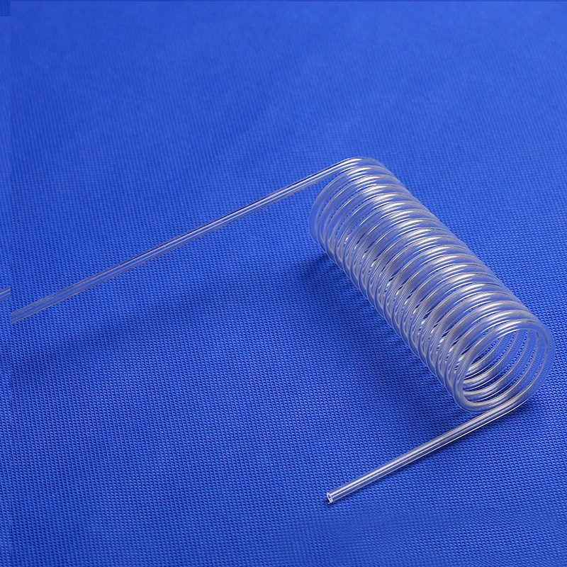
Precision Laser Micro-Channeling & Drilling: In DNA sequencing apparatus and microfluidic reaction chips, traditional diamond drilling is too blunt to yield microscale channels. Advanced manufacturers now deploy femtosecond laser machining followed by fluorinated vapor polishing to create high-aspect-ratio holes (φ ≤ 50 μm) and micro-grooves possessing pristine, fire-polished walls for undisturbed capillary dynamics.
Integrated High-Frequency RF Packaging: Due to an ultra-low dielectric constant (εr ≈ 3.78 at 1 MHz) and exceptionally low dielectric loss tangent (tanδ < 0.0001), quartz glass substrates are replacing alumina and silicon in 5G/6G millimeter-wave packaging and quantum computing interposers, where electromagnetic dispersion must be eliminated.
Frequently Asked Questions
B2B Quartz Substrate Sourcing & Engineering FAQ
Direct technical answers addressing critical supplier vetting, tolerances, export handling, and material validation queries.
How do you evaluate and control internal residual stress in quartz substrates?
Residual thermal stress is the primary cause of spontaneous substrate fracture during laser processing or vacuum cycling. Lovri Quartz subjects all substrates to a computer-controlled 1,180°C annealing and slow cooling cycle, followed by 100% inspection using a polarization stress birefringence analyzer (dual-polarizer system) verifying optical retardation below 10 nm/cm.
Can you execute custom geometries from CAD files (STEP, DWG, DXF)?
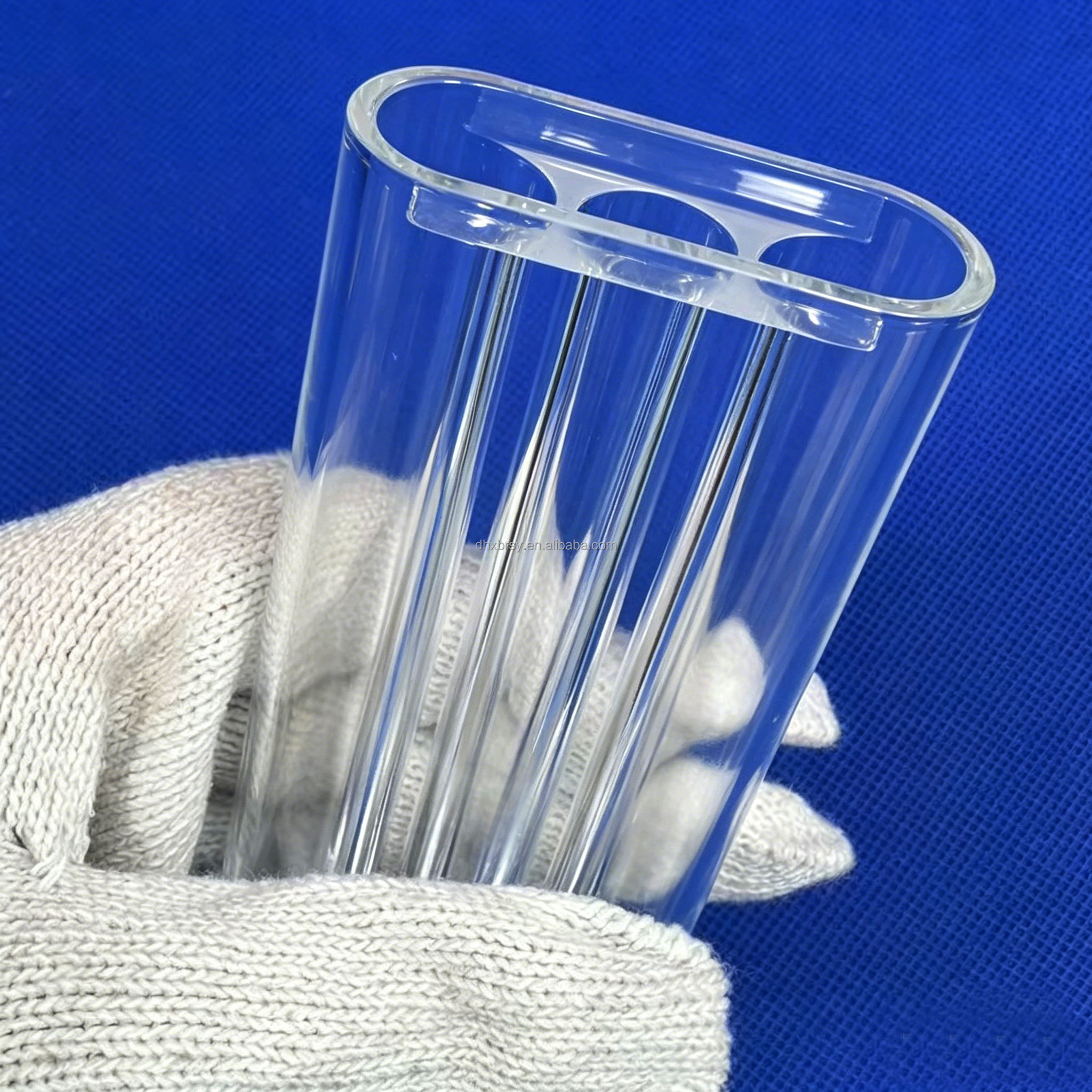
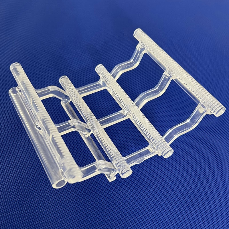
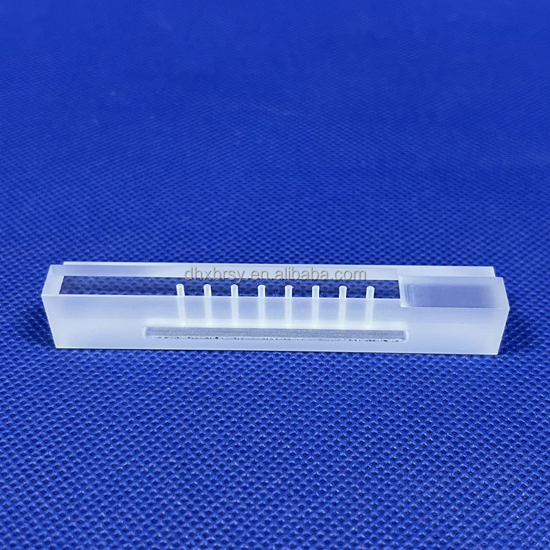
Yes. Our CNC milling center utilizes multi-axis diamond machining systems calibrated specifically for brittle glassy materials. We fabricate complex custom slots, through-holes, stepped edges, bevels, V-grooves, and hollow manifolds directly from your STEP, DWG, or PDF drawings with dimensional tolerances held to ±0.005 mm.
What is your Minimum Order Quantity (MOQ) for custom prototypes?
We maintain an engineering-first prototype policy. For custom dimensions, wafer boats, or non-standard substrate discs, we accept prototype batch orders from as low as 1 to 5 pieces. Once physical performance and tolerances are validated by your engineers, production seamlessly scales to thousands of production units monthly.
What packaging protocols protect fragile quartz substrates during global air freight?
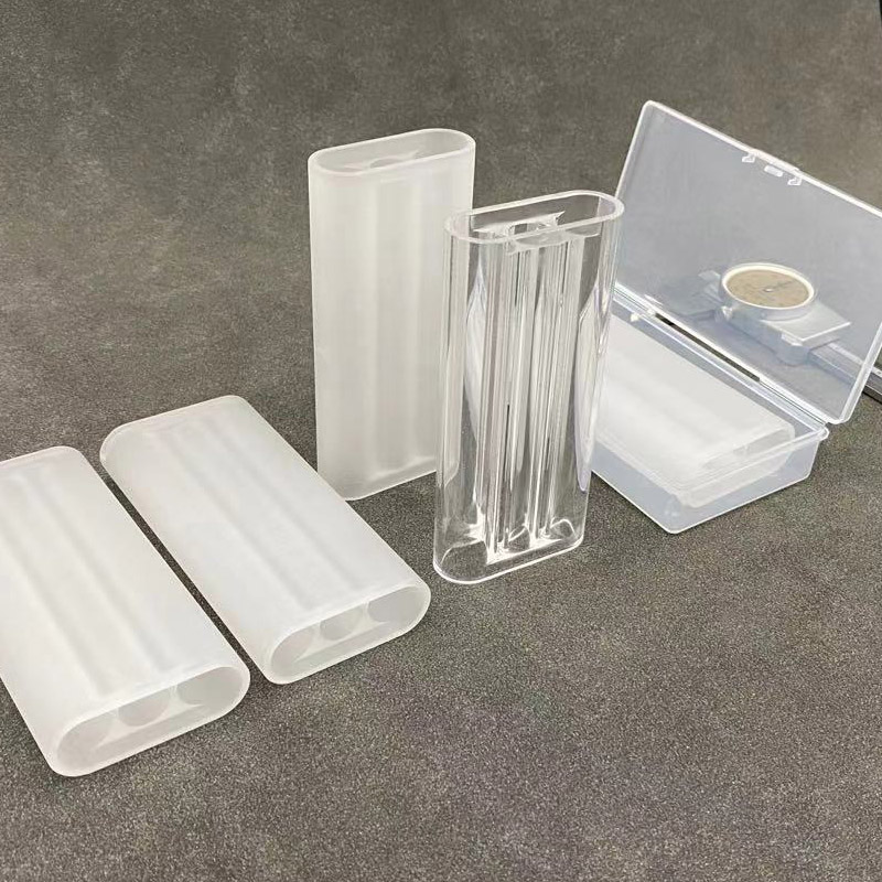
Each optical plate or substrate undergoes ultra-pure cleanroom wiping, individual vacuum-sealing in antistatic lint-free PET pouches, placement inside precision cut EVA shock-absorption molds, and packing within reinforced dual-wall corrugated cartons or fumigated export wooden crates capable of withstanding rough multi-modal transport.
What are the maximum operational temperatures for your fused quartz substrates?
Transparent fused quartz sustains continuous long-term operations at up to 1,100°C and intermittent peak excursions up to 1,300°C. The softening point occurs at 1,730°C. For prolonged thermal stability, avoid contact with alkaline dust or direct fingerprint oils at elevated temperatures, which can initiate surface devitrification.
How do you guarantee chemical purity and trace metal compliance?
Our raw natural and synthetic silica batches are monitored via Inductively Coupled Plasma Mass Spectrometry (ICP-MS). Each production shipment is furnished with comprehensive chemical composition certifications validating that elemental concentrations of Fe, Al, Cu, Cr, and Ni remain under specified threshold limits to satisfy RoHS/REACH compliance.
Ready to Engineer Your Custom Quartz Substrate Solution?
Consult directly with our senior quartz materials application engineers. Whether you need an immediate prototype quote, custom CNC feasibility feedback, or bulk factory production terms, our technical team replies within 24 hours.